STMicroelectronics HCC4724B
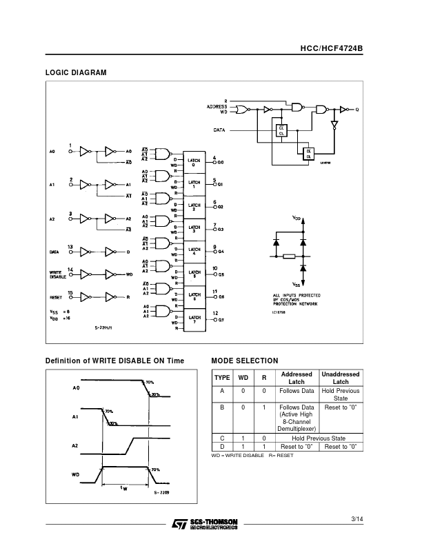
The HCC/HCF4724B 8-bit addressable latch is a serial-input, parallel-output storage register that can perform a variety of functions. When WRITE DISABLE is high, data entry is inhibited however, all 8 outputs can be continuously read independent of WRITE DISABLE and address inputs. When RESET is at a high level, and WRITE DISABLE is at a low level, the latch acts as a 1-of-8 demultiplexer ; the bit that is addressed has an active output which follows the data input, while all unaddressed bits are held to a logic ” 0 ” level.
| Part No. |
HCC4724B |
| Datasheet |
HCC4724B
Download
|
| Manufacturer |
 STMicroelectronics |
| Description |
8 BIT ADDRESSABLE LATCH |
| Buy |
Stock & Price
|
DESCRIPTION
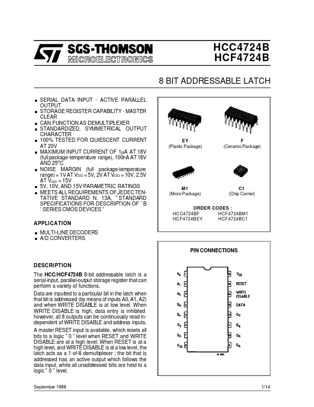
OF ’ B ’ SERIES CMOS DEVICES ” EY (Plastic Package) F (Ceramic Package) M1 (Micro Package) C1 (Chip Carrier) ORDER CODES : HCC4724BF HCF4724BM1 HCF4724BEY HCF4724BC1 APPLICATION MULTI-LINE DECODERS A/D CONVERTERS PIN CONNECTIONS DESCRIPTION
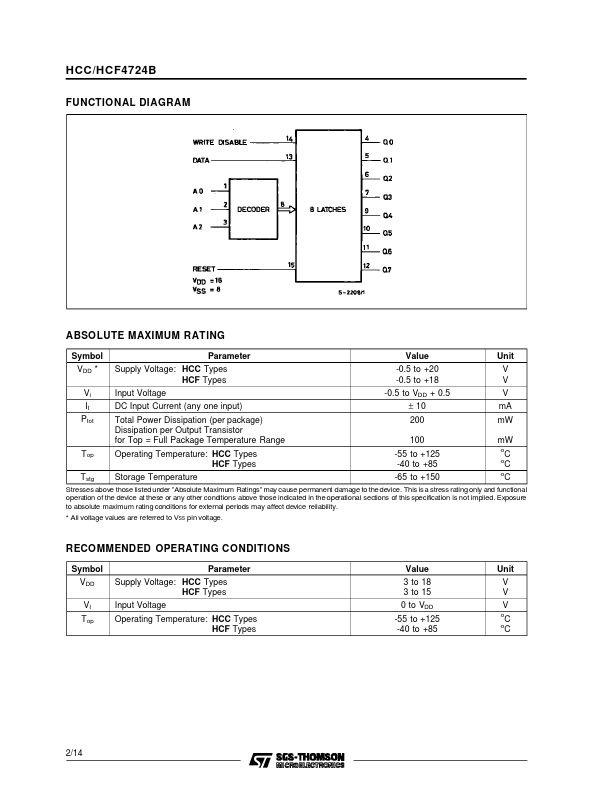
Data are inputted to a particular bit in the latch when that bit is addressed (by means of inputs A0, A1, A2) and when WRITE DISABLE is at low level. A master RESET input is available, which resets all bits to a logic ” 0 ” level when RESET and WRITE DISABLE are at a high level. September 1988 1/14 HCC/HCF4724B FUNCTIONAL DIAGRAM ABSOLUTE MAXIMUM RATING Symbol VDD * Vi II Ptot Parameter Supply Voltage: HCC Types HCF Types Input Voltage DC Input Current (any one input) Total Power Dissipation (per package) Dissipation per Output Transistor for Top = Full Package Temperature Range Operating Temperature: HCC Types HCF Types Storage Temperature Value -0.5 to +20 -0.5 to +18 -0.5 to VDD + 0.5 ± 10 200 100 -55 to +125 -40 to +85 -65 to +150 Unit V V V mA mW mW o o o Top Tstg C C C Stresses above those listed under ”ABSOLUTE MAXIMUM RATINGS
” may cause permanent damage to the device.