HCF4007UB
HCF4007UB is DUAL COMPLEMENTARY PAIR PLUS INVERTER manufactured by STMicroelectronics.
DUAL PLEMENTARY PAIR PLUS INVERTER s STANDARDIZED SYMMETRICAL OUTPUT
CHARACTERISTICS s MEDIUM SPEED OPERATION t PD = 30ns (Typ.) AT 10V s QUIESCENT CURRENT SPECIFIED UP TO
)20V t(ss 5V, 10V AND 15V PARAMETRIC RATINGS s INPUT LEAKAGE CURRENT uc II = 100n A (MAX) AT VDD = 18V TA = 25°C ds 100% TESTED FOR QUIESCENT CURRENT Pro DESCRIPTION
The HCF4007UB is a monolithic integrated circuit tefabricated in Metal Oxide Semiconductor letechnology available in DIP and SOP packages. o The HCF4007UB type is prised of three sn-channel and three p-channel enhancement type b MOS transistors. The transistor elements are Oaccessible through the package terminals to -provide a convenient means for constructing the )various typical circuits as shown in typical
DIP SOP
ORDER CODES
PACKAGE
TUBE
DIP SOP
HCF4007UBEY HCF4007UBM1
T&R HCF4007UM013TR applications. More plex functions are possible using multiple packages. Number shown in parentheses indicate terminals that are connected together to form the various configuration listed.
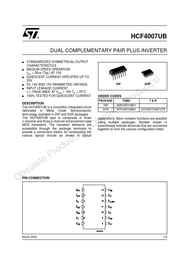
Obsolete Product(s PIN CONNECTION
March 2004
1/9
INPUT EQUIVALENT CIRCUIT
PIN DESCRIPTION
PIN N°
SYMBOL NAME AND FUNCTION
2, 11
SP2, SP3
Source Connections to 2nd and 3rd p-channel transistors
13, 1
DP1, DP2
Drain Connections from the 1st and 2nd p-channel transistors
Drain Connections from 8, 5 DN1, DN2 the 1st and 2nd n-channel transistors lete Product(s)LOGIC DIAGRAM
4, 9 12
6, 3, 10 7 14
SN2, SN3 DN/P3
G1 to G3 VSS VDD
Source Connections to the 2nd and 3rd n-channel mon connection to the 3rd p-channel and n-channel transistor...