DESCRIPTION
OF B SERIES CMOS DEVICES” no new data is netered. In either case, the contents of any word may be accessed via the read address lines independent of the state of the CLOCK input. EY (Plastic Package) F (Ceramic Package) M1 (Micro Package) C1 (Chip Carrier) ORDER CODES : HCC40108BF HCF40108BM1 HCF40108BEY HCF40108BC1 PIN CONNECTIONS DESCRIPTION
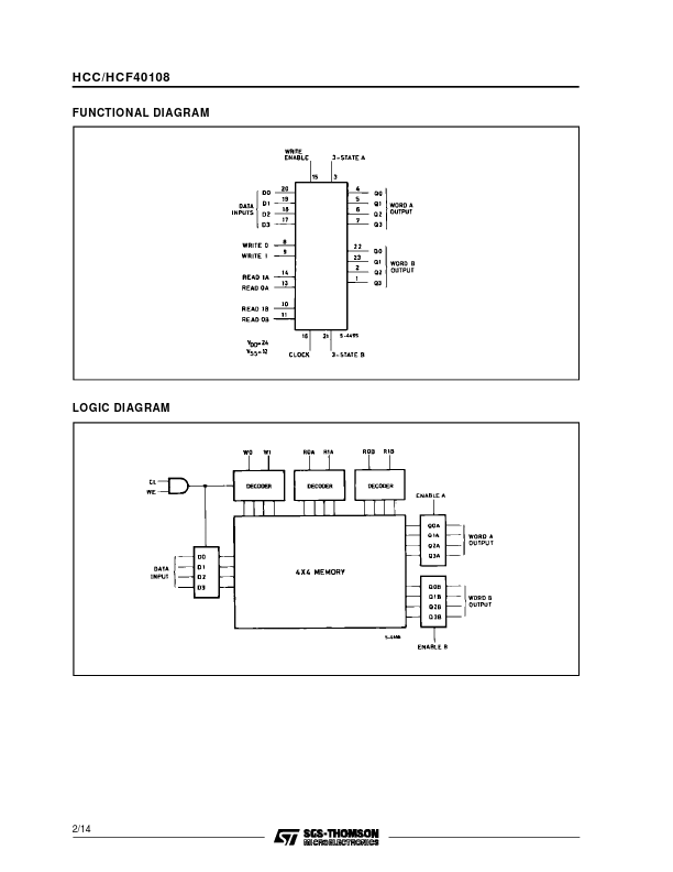
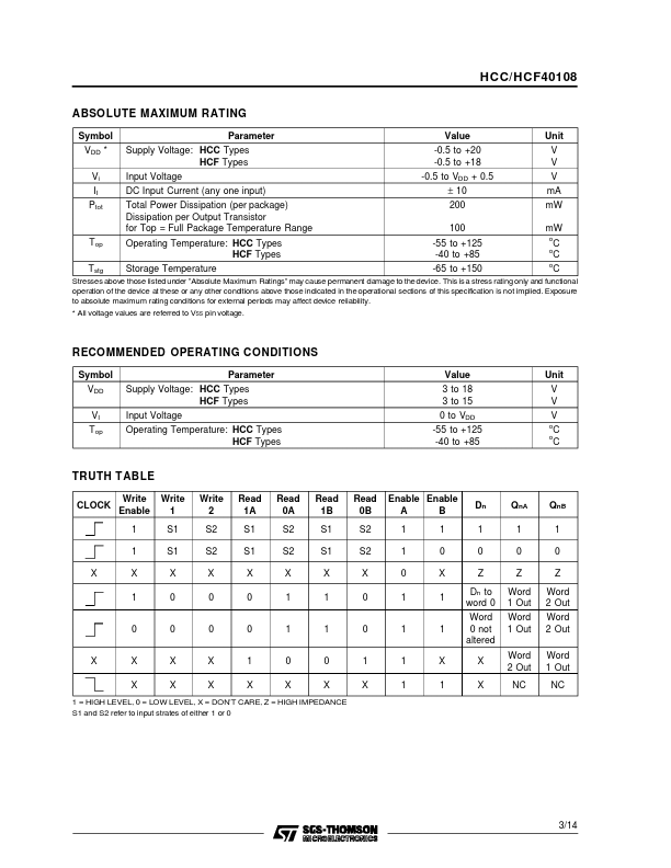
When the ENABLE input is low, the corresponding output bus is switched, independently of the clock, to a high impedance state. The high impedance third state provides the outputs with the capability of being connected to the bus lines in a bus organized system without the need for interface or pull-up components. When the WRITE ENABLE input is high, all data input lines are latched on the positive transition of the CLOCK and the data is entered into the word selected by the write address lines. When WRITE ENABLE is low, the CLOCK is inhibited and September 1988 1/14 HCC/HCF40108 FUNCTIONAL DIAGRAM LOGIC DIAGRAM 2/14 HCC/HCF40108 ABSOL... STMicroelectronics