DESCRIPTION
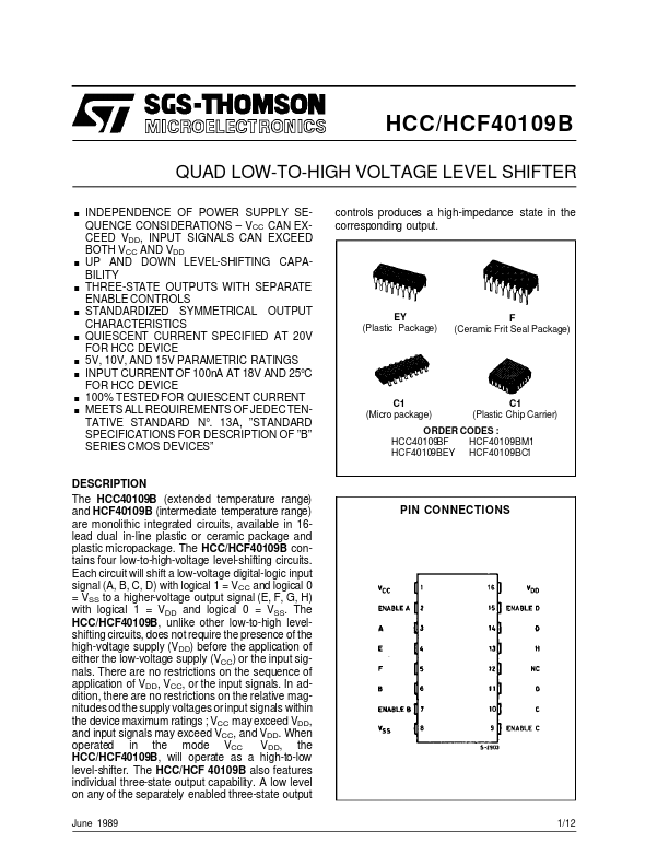
OF ”B” SERIES CMOS DEVICES” controls produces a high-impedance state in the corresponding output. EY (Plastic Package) F (Ceramic Frit Seal Package) C1 (Micro package) C1 (Plastic Chip Carrier) ORDER CODES : HCC40109BF HCF40109BM1 HCF40109BEY HCF40109BC1 DESCRIPTION
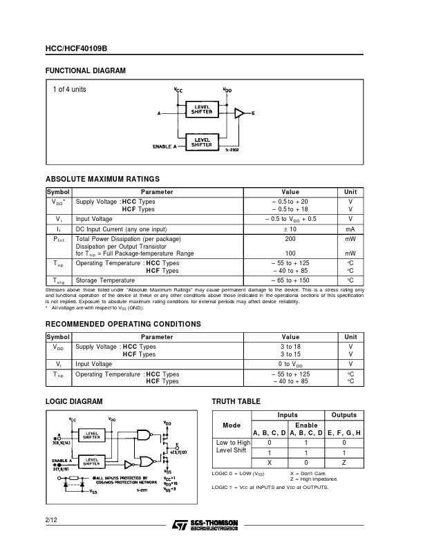
Each circuit will shift a low-voltage digital-logic input signal (A, B, C, D) with logical 1 = VCC and logical 0 = VSS to a higher-voltage output signal (E, F, G, H) with logical 1 = VDD and logical 0 = VSS. The HCC/HCF40109B , unlike other low-to-high levelshifting circuits, does not require the presence of the high-voltage supply (VDD) before the application of either the low-voltage supply (VCC) or the input signals. There are no restrictions on the sequence of application of VDD, VCC, or the input signals. In addition, there are no restrictions on the relative magnitudes od the supply voltages or input signals within the device maximum ratings ; VCC may exceed VDD, and input signals may exceed VCC, and VDD. When operated in the mode VCC VDD, the HCC/HCF40109B , will operate as a high-to-low level-shifter. STMicroelectronics