DESCRIPTION
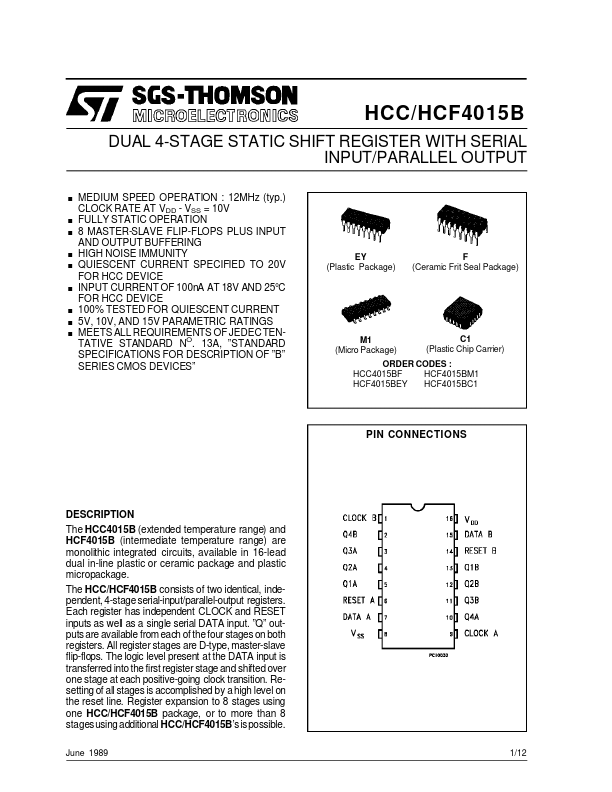
OF ”B” SERIES CMOS DEVICES” EY (Plastic Package) F (Ceramic Frit Seal Package) M1 (Micro Package) C1 (Plastic Chip Carrier) ORDER CODES : HCC4015BF HCF4015BM1 HCF4015BEY HCF4015BC1 PIN CONNECTIONS DESCRIPTION
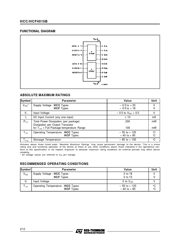
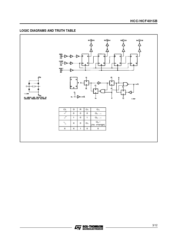
Each register has independent CLOCK and RESET inputs as well as a single serial DATA input. ”Q” outputs are available from each of the four stages on both registers. All register stages are D-type, master-slave flip-flops. The logic level present at the DATA input is transferred into the first register stage and shifted over one stage at each positive-going clock transition. Resetting of all stages is accomplished by a high level on the reset line. Register expansion to 8 stages using one HCC/HCF4015B package, or to more than 8 stages using additional HCC/HCF4015B’s is possible. June 1989 1/12 HCC/HCF4015B FUNCTIONAL DIAGRAM ABSOLUTE MAXIMUM RATINGS
Symbol V DD * Vi II Pto t Parameter Supply Voltage : HC C Types H CF Types Input Voltage DC Input Current (any one input)... STMicroelectronics