DESCRIPTION
OF ”B” SERIES CMOS DEVICES”. EY (Plastic Package) F (Ceramic Frit Seal Package) M1 (Micro Package) C1 (Plastic Chip Carrier) ORDER CODES : HCC4027BF HCF4027BM1 HCF4027BEY HCF4027BC1 PIN CONNECTIONS DESCRIPTION
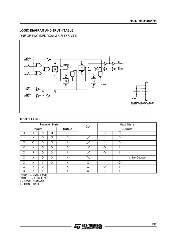
Each flip-flop has provisions for individual J, K, Set, Reset, and Clock input signals, Buffered Q and Q signals are provided as outputs. This input-output arrangement provides for compatible operation with the HCC/HCF4013B dual D-type flip-flop. The HCC/HCF4027B is useful in performing control, register, and toggle functions. Logic levels present at the J and K inputs along with internal self-steering control the state of each flip-flop ; changes in the flipflop state are synchronous with the positive-going transition of the clock pulse. Set and reset functions are independent of the clock and are initiated when a high level signal is present at either the Set or Reset input. June 1989 1/12 HCC/HCF4027B FUNCTIONAL DIAGRAM ABSOLUTE MAXIMUM RATINGS
Symbol V DD* Vi II P... STMicroelectronics