DESCRIPTION
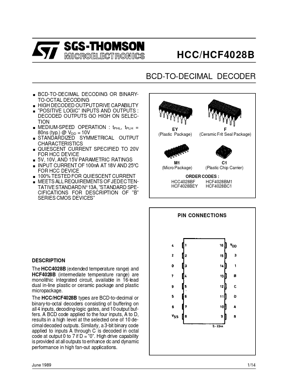
OF ”B” SERIES CMOS DEVICES” EY (Plastic Package) F (Ceramic Frit Seal Package) M1 (Micro Package) C1 (Plastic Chip Carrier) ORDER CODES : HCC4028BF HCF4028BM1 HCF4028BEY HCF4028BC1 PIN CONNECTIONS DESCRIPTION
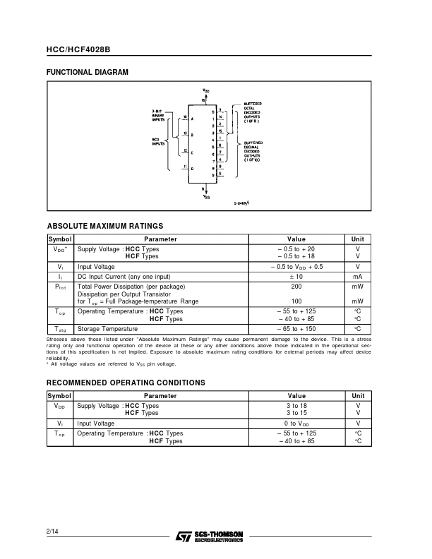
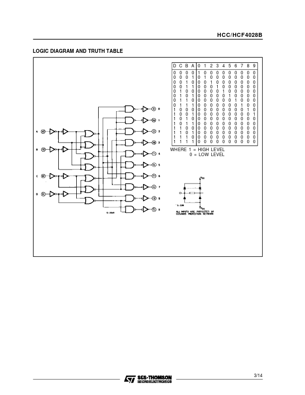
A BCD code applied to the four inputs, A to D, results in a high level at the selected one of 10 decimal decoded outputs. Similarly, a 3-bit binary code applied to inputs A through C is decoded in octal code at output 0 to 7 if D = ”0”. High drive capability is provided at all outputs to enhance dc and dynamic performance in high fan-out applications. June 1989 1/14 HCC/HCF4028B FUNCTIONAL DIAGRAM ABSOLUTE MAXIMUM RATINGS
Symbol V DD * Vi II Pt o t Parameter Supply Voltage : HC C Types H C F Types Input Voltage DC Input Current (any one input) Total Power Dissipation (per package) Dissipation per Output Transistor for T o p = Full Package-temperature Range Operating Temperature : HCC Types H CF Types Storage Temperature Value – 0.5 to + 20 – 0.5 to + 18 – 0.5 to V DD +... STMicroelectronics