DESCRIPTION
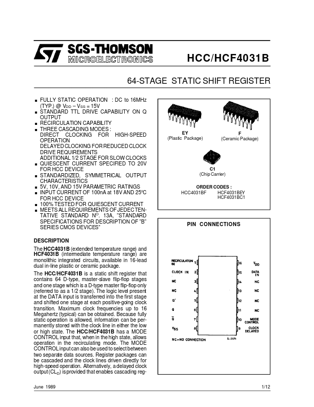
OF ”B” SERIES CMOS DEVICES” EY (Plastic Package) F (Ceramic Package) C1 (Chip Carrier) ORDER CODES : HCC4031BF HCF4031BEY HCF4031BC1 PIN CONNECTIONS DESCRIPTION
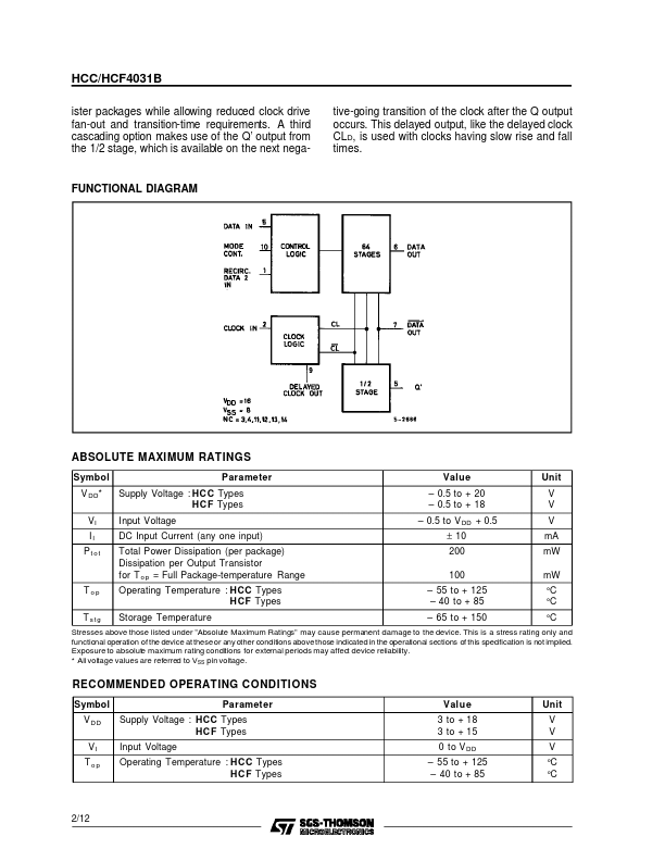
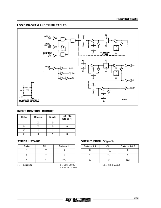
The logic level present at the DATA input is transferred into the first stage and shifted one stage at each positive-going clock transition. Maximum clock frequencies up to 16 Megahertz (typical) can be obtained. Because fully static operation is allowed, information can be permanently stored with the clock line in either the low or high state. The HCC/HCF4031B has a MODE CONTROL input that, when in the high state, allows operation in the recirculating mode. The MODE CONTROL input can also be used to select between two separate data sources. Register packages can be cascaded and the clock lines driven directly for high-speed operation. Alternatively, a delayed clock output(CLD) is provided that enables cascading regJune 1989 1/12 HCC/HCF4031B ister packages while allowing reduced clock drive fan-out and transition-time requirements. STMicroelectronics