HCF4042B
HCF4042B is QUAD CLOCKED D LATCH manufactured by STMicroelectronics.
HCC/HCF4042B
QUAD CLOCKED ”D” LATCH
- . . . . .
CLOCK POLARITY CONTROL Q AND Q OUTPUTS MON CLOCK LOW POWER TTL PATIBLE STANDARDIZED SYMMETRICAL OUTPUT CHARACTERISTICS QUIESCENT CURRENT SPECIFIED TO 20V FOR HCC DEVICE 5V, 10V, AND 15V PARAMETRIC RATINGS INPUT CURRENT OF 100n A AT 18V AND 25°C FOR HCC DEVICE 100% TESTED FOR QUIESCENT CURRENT MEETS ALL REQUIREMENTS OF JEDEC TENTATIVE STANDARD N° 13A, ”STANDARD SPECIFICATIONS FOR DESCRIPTION OF ”B” SERIES CMOS DEVICES”
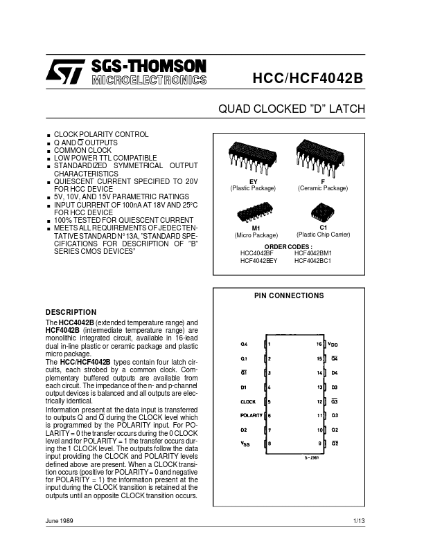
EY (Plastic Package)
F (Ceramic Package)
M1 (Micro Package)
C1 (Plastic Chip Carrier)
ORDER CODES : HCC4042BF HCF4042BM1 HCF4042BEY HCF4042BC1
PIN CONNECTIONS DESCRIPTION The HCC4042B (extended temperature range) and HCF4042B (intermediate temperature range) are monolithic integrated circuit, available in 16-lead dual in-line plastic or ceramic package and plastic micro package. The HCC/HCF4042B types contain four latch circuits, each strobed by a mon clock. plementary buffered outputs are available from each circuit. The impedance of the n- and p-channel output devices is balanced and all outputs are electrically identical. Information present at the data input is transferred to outputs Q and Q during the CLOCK level which is programmed by the POLARITY input. For POLARITY = 0 the transfer occurs during the 0 CLOCK level and for POLARITY = 1 the transfer occurs during the 1 CLOCK level. The outputs follow the data input providing the CLOCK and POLARITY levels defined above are present. When a CLOCK transition occurs (positive for POLARITY = 0 and negative for POLARITY = 1) the information present at the input during the CLOCK transition is retained at the outputs until an opposite CLOCK transition occurs.
June 1989
1/13
HCC/HCF4042B
FUNCTIONAL...