DESCRIPTION
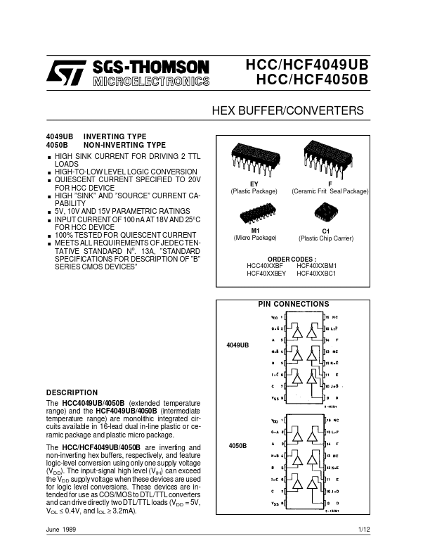
OF ”B” SERIES CMOS DEVICES” EY (Plastic Package) F (Ceramic Frit Seal Package) M1 (Micro Package) C1 (Plastic Chip Carrier) ORDER CODES : HCC40XXBF HCF40XXBM1 HCF40XXBEY HCF40XXBC1 PIN CONNECTIONS 4049UB DESCRIPTION
The HCC4049UB/4050B (extended temperature range) and These devices are intended for use as COS/MOS to DTL/TTL converters and can drive directly two DTL/TTL loads (VDD = 5V, VOL ≤ 0.4V, and IOL ≥ 3.2mA). June 1989 4050B 1/12 HCC/HCF4049UB/4050B SCHEMATIC DIAGRAMS (1 of 6 identical units) 4049UB 4050B ABSOLUTE MAXIMUM RATINGS
Symbol V DD* Vi II Pt ot Parameter Supply Voltage : HC C Types H C F Types Input Voltage DC Input Current (any one input) Total Power Dissipation (per package) Dissipation per Output Transistor for T o p = Full Package-temperature Range Operating Temperature : HCC Types H CF Types Storage Temperature Value – 0.5 to + 20 – 0.5 to + 18 – 0.5 to V DD + 0.5 ± 10 200 100 – 55 to + 125 – 40 to + 85 – 65 to + 150 Unit V V V mA mW mW °C °C °C Top Tstg Stresses above those listed under ”ABSOLUTE MAXIMUM RATINGS
” may cause permanent damage to the device. STMicroelectronics