DESCRIPTION
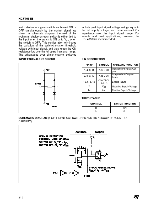
In addition, the ON resistance is relatively constant over the full input signal range. The HCF4066B consists of four independent bilateral switches. A single control signal is required per switch. Both the p March 2004 1/10 HCF4066B and n device in a given switch are biased ON or OFF simultaneously by the control signal. As shown in schematic diagram, the well of the n-channel device on each switch is either tied to the input when the switch is ON or to VSS when the switch is OFF. This configuration eliminates the variation of the switch-transistor threshold voltage with input signal, and thus keeps the ON resistance low over the full operating signal range. The advantages over single channel switches INPUT EQUIVALENT CIRCUIT include peak input signal voltage swings equal to the full supply voltage, and more constant ON impedance over the input signal range. For sample and hold applications, however, the HCF4016B is recommended. PIN DESCRIPTION
PIN N° 1, 4, 8, 11 2, 3, 9,... STMicroelectronics