DESCRIPTION
OF B SERIES CMOS DEVICES" DIP SOP ORDER CODES PACKAGE DIP SOP TUBE HCF4086BEY HCF4086BM1 T&R HCF4086M013TR DESCRIPTION
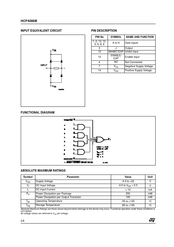
HCF4086B contains one 4-wide 2-input AND-OR INVERT gates with an INHIBIT EXP input and an ENABLE/EXP input. INHIBIT/EXP is tied to VSS and ENABLE/EXP to VDD. For a 4 wide A-O-I function. PIN CONNECTION September 2002 1/8 HCF4086B INPUT EQUIVALENT CIRCUIT PIN DESCRIPTION
PIN No SYMBOL NAME AND FUNCTION Data Inputs Output Inhibit Input Enable Input Not Connected Negative Supply Voltage Positive Supply Voltage 1, 2, 12, 13, A to H 5, 6, 8, 9 3 J 10 INHIBIT/EXP ENABLE/ 10 EXP NC 4 7 14 VSS VDD FUNCTIONAL DIAGRAM ABSOLUTE MAXIMUM RATINGS
Symbol VDD VI II PD Top Tstg Supply Voltage DC Input Voltage DC Input Current Power Dissipation per Package Power Dissipation per Output Transistor Operating Temperature Storage Temperature Parameter Value -0.5 to +22 -0.5 to VDD + 0.5 ± 10 200 100 -55 to +125 -65 to +150 Unit V V mA mW mW °C °C ABSOLUTE MAXIMUM RATINGS
are those values beyond which damage to the device may occur. STMicroelectronics