STMicroelectronics HCF4093B
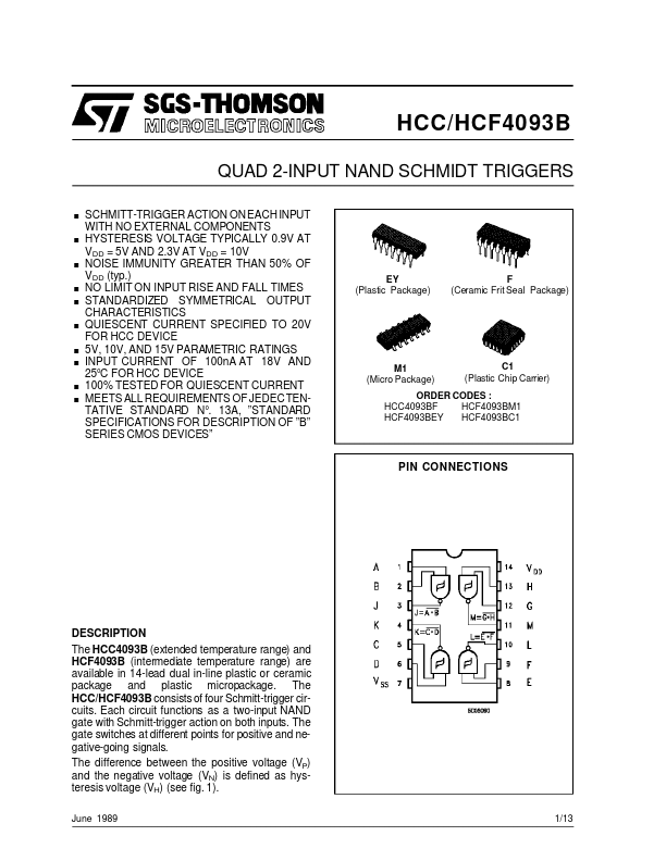
The HCC4093B (extended temperature range) and HCF4093B (intermediate temperature range) are available in 14-lead dual in-line plastic or ceramic package and plastic micropackage. The HCC/HCF4093B consists of four Schmitt-trigger circuits.| Part No. | HCF4093B |
|---|---|
| Datasheet | HCF4093B Download |
| Manufacturer |  STMicroelectronics |
| Description | QUAD 2-INPUT NAND SCHMIDT TRIGGERS |
| Buy | Stock & Price |
DESCRIPTION
OF ”B” SERIES CMOS DEVICES” EY (Plastic Package) F (Ceramic Frit Seal Package) M1 (Micro Package) C1 (Plastic Chip Carrier) ORDER CODES : HCC4093BF HCF4093BM1 HCF4093BEY HCF4093BC1 PIN CONNECTIONSDESCRIPTION
Each circuit functions as a two-input NAND gate with Schmitt-trigger action on both inputs. The gate switches at different points for positive and negative-going signals. The difference between the positive voltage (VP) and the negative voltage (VN) is defined as hysteresis voltage (VH) (see fig. 1). June 1989 1/13 HCC/HCF4093B FUNCTIONAL DIAGRAM 1 of 4 Schmitt triggersABSOLUTE MAXIMUM RATINGS
Symbol V DD * VI II Pto t Parameter Supply Voltage : HC C Types H C F Types Input Voltage DC Input Current (any one input) Total Power Dissipation (per package) Dissipation per Output Transistor for T o p = Full Package-temperature Range Operating Temperature : HCC Types H CF Types Storage Temperature Value – 0.5 to + 20 – 0.5 to + 18 – 0.5 to V DD + 0.5 ± 10 200 100 – 55 to + 1...