DESCRIPTION
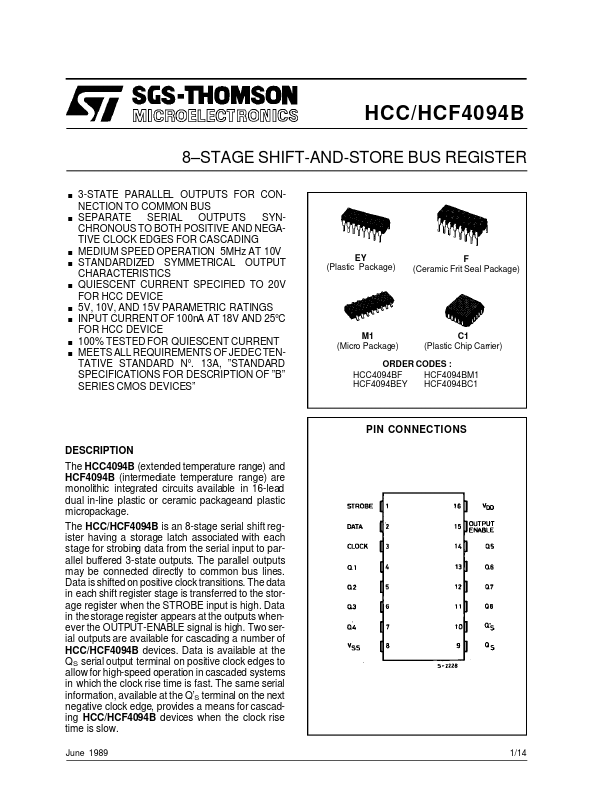
OF ”B” SERIES CMOS DEVICES” EY (Plastic Package) F (Ceramic Frit Seal Package) M1 (Micro Package) C1 (Plastic Chip Carrier) ORDER CODES : HCC4094BF HCF4094BM1 HCF4094BEY HCF4094BC1 PIN CONNECTIONS DESCRIPTION
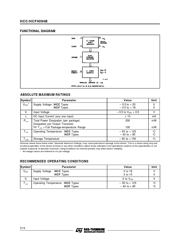
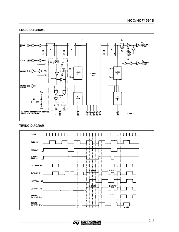
The parallel outputs may be connected directly to common bus lines. Data is shifted on positive clock transitions. The data in each shift register stage is transferred to the storage register when the STROBE input is high. Data in the storage register appears at the outputs whenever the OUTPUT-ENABLE signal is high. Two serial outputs are available for cascading a number of HCC/HCF4094B devices. Data is available at the QS serial output terminal on positive clock edges to allow for high-speed operation in cascaded systems in which the clock rise time is fast. The same serial information, available at the Q’S terminal on the next negative clock edge, provides a means for cascading HCC/HCF4094B devices when the clock rise time is slow. June 1989 1/14 HCC/HCF4094B FUNCTIO... STMicroelectronics