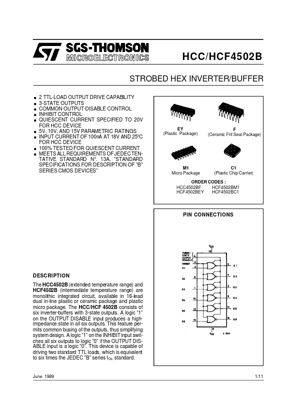
DESCRIPTION
OF ”B” SERIES CMOS DEVICES” EY (Plastic Package) F (Ceramic Frit Seal Package) M1 Micro Package C1 (Plastic Chip Carrier) ORDER CODES : HCC4502BF HCF4502BM1 HCF4502BEY HCF4502BC1 PIN CONNECTIONS DESCRIPTION
A logic ”1” on the OUTPUT DISABLE input produces a highimpedance state in all six outputs. This feature permits common busing of the outputs, thus simplifying system design. A logic ”1” on the INHIBIT input switches all six outputs to logic ”0” if the OUTPUT DISABLE input is a logic ”0”. This device is capable of driving two standard TTL loads, which is equivalent to six times the JEDEC ”B” series IOL standard. June 1989 1/11 HCC/HCF4502B ABSOLUTE MAXIMUM RATINGS
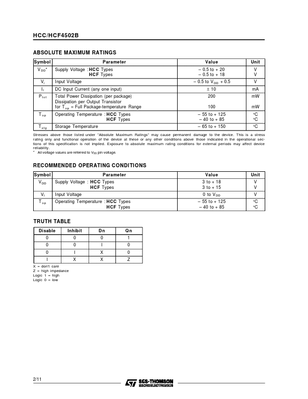
Symbol V DD* Vi II Pt ot Parameter Supply Voltage : HC C Types H C F Types Input Voltage DC Input Current (any one input) Total Power Dissipation (per package) Dissipation per Output Transistor for T o p = Full Package-temperature Range Operating Temperature : HCC Types H CF Types Storage Temperature Value – 0.5... STMicroelectronics