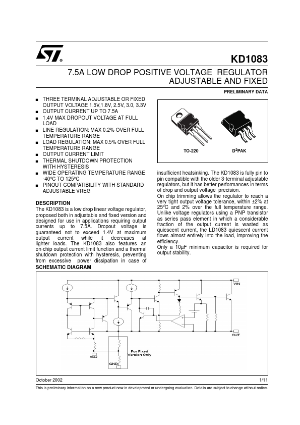
DESCRIPTION
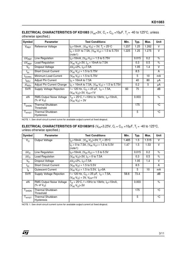
Dropout voltage is guaranteed not to exceed 1.4V at maximum output current while it decreases at lighter loads. On chip trimming allows the regulator to reach a very tight output voltage tolerance, within ±2% at 25°C and 2% over the full temperature range. Unlike voltage regulators using a PNP transistor as series pass element in which a considerable fraction of the output current is wasted as quiescent current, the LD1083 quiescent current flows almost entirely into the load, improving the efficiency. Only a 10µF minimum capacitor is required for output stability. October 2002 1/11 This is preliminary information on a new product now in development or undergoing evaluation. Details are subject to change without notice. KD1083 ABSOLUTE MAXIMUM RATINGS
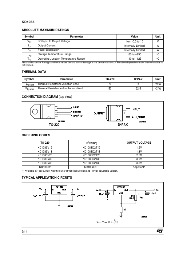
Symbol VIN IO PD Tstg Top DC Input to Output Voltage Output Current Power Dissipation Storage Temperature Range Operating Junction Temperature Range Parameter Value from -0.3 to 10 Internally Limited Internally Limited -55 to +150 -40 to +125 Unit V A W °C °C ABSOLUTE MAXIMUM RATINGS
are those values beyond which damage to the device may occur. STMicroelectronics