L149
L149 is 4A LINEAR DRIVER manufactured by STMicroelectronics.
DESCRIPTION
The L149 is a general purpose power booster in Pentawatt ® package consisting of a quasi-plentary darlington output stage with the associated biasing system an inhibit facility. The device is particularly suited for use with an operational amplifier inside a closed loop configuration to increase output current. ABSOLUTE MAXIMUM RATINGS
Symbol Vs Vi V5
- V4 V4
- V3 Io Iο VINH Ptot Supply Voltage Input Voltage Upper Power Transistor VCE Lower Power Transistor VCE DC Output Current Peak Output Current (internally limited) Input Inhibit Voltage Total Power Dissipation at Tcase = 75 °C) 40 40 3 4
- Vs + 5
- Vs
- 1.5 25 Parameter Value ±20 Unit V Vs V V A A V V W
Pentawatt®
ORDER CODE : L149V
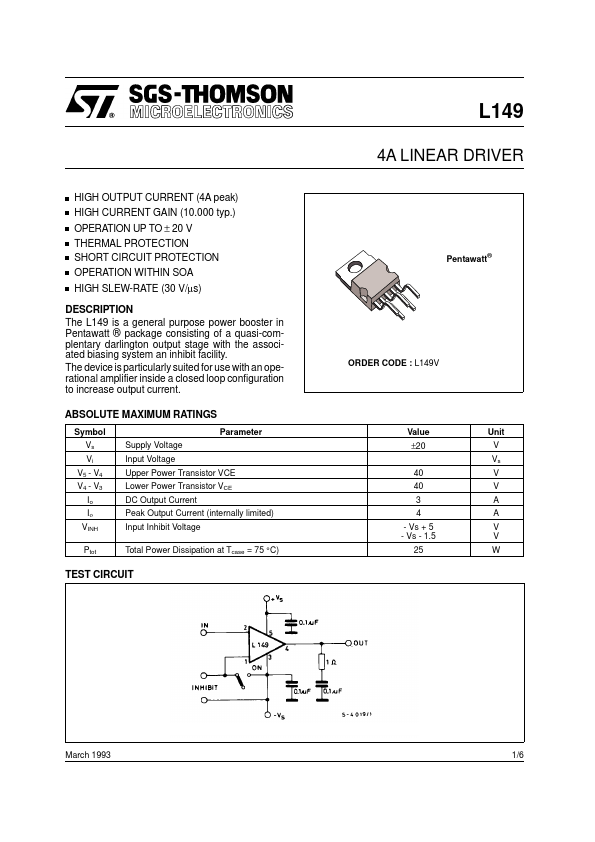
TEST CIRCUIT
March 1993
1/6
CONNECTION DIAGRAM (top view)
SCHEMATIC DIAGRAM
2/6
THERMAL DATA
Symbol Rth-j-case Thermal resistance junction-case Parameter max Value 3 Unit °C/W
ELECTRICAL CHARACTERISTICS (Tj = 25 °C, Vs = ± 16V)
Symbol Vs Id Iin h FE GV VCEsat Vos VINH Parameter Supply Voltage Quiescent Drain Current Input current DC current drain Voltage gain Saturation voltage (for each transistor) Input offset voltage Inhibit input voltage (pins 1-3) Vs = ± 16 V Vs = ± 16 V Vs = ± 16 V Vs = ± 16 V Io = 3A Vs = ± 16 V ON condition OFF condition RINH SR B Inhibit input resistance Slew rate Power bandwidth Vo = ± 10V, d = 1%, RL = 8Ω ± 1.8 2.0 30 200 Vi = 0V Io = 3A Io = 1.5A 6000 30 200 10000 1 3.5 0.3 ± 0.3 400 Test conditions Min. Typ. Max. ± 20 Unit V m A µA V V V KΩ V/µs KHZ
APPLICATION INFORMATION Figure 1. High slew-rate power operational amplifier (SR = 13V/µs)
3/6
Figure 2. Maximum saturation voltage vs. output current. Figure 3. Current limiting characteristics.
Fi gure 4: Suppl y voltage rejection vs. frequency.
Figure 5: Distorsion vs. output power (f = 1KHz).
Figure 6. Distorsion vs. output power (f = 1KHz).
Figure 7. Output power vs. supply voltage.
4/6
PENTAWATT PACKAGE MECHANICAL DATA
DIM. MIN. A C D D1 E F F1 G G1 H2...