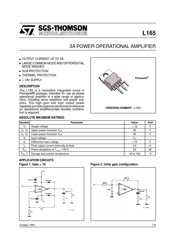
DESCRIPTION
ABSOLUTE MAXIMUM RATINGS
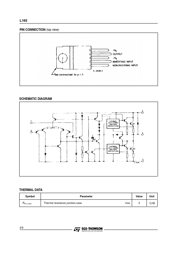
Symbol Vs Supply voltage V5 V4 Upper power transistor VCE V4 V3 Lower power transistor VCE Vi Input voltage Vj Differential input voltage Io Ptot Tstg, Tj Power dissipation at Tcase = 90°C Storage and junction temperature Parameter Value ± 18 36 36 Vs ± 15 3.5 20 -40 to 150 Unit V V V V A W °C Pentawatt® ORDERING NUMBER : L165V Peak output current (internally limited) APPLICATION CIRCUITS Figure 1. Gain > 10. Figure 2. Unity gain configuration. October 1991 1/9 L165 PIN CONNECTION (top view) SCHEMATIC DIAGRAM THERMAL DATA Symbol Rth-j-case Parameter Thermal resistance junction-case max Value 3 Unit °C/W 2/9 L165 ELECTRICAL CHARACTERISTICS
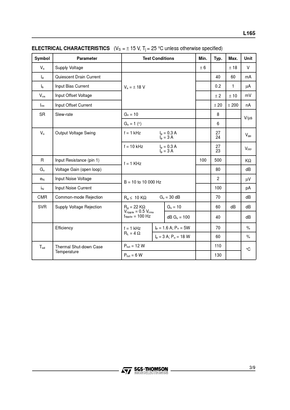
(VS = ± 15 V, Tj = 25 °C unless otherwise specified) Symbol Vs Id Ib Vos Ios SR Parameter Supply Voltage Quiescent Drain Current Input Bias Current Input Offset Voltage Input Offset Current Slew-rate Gv = 10 Gv = 1 (°) Vo Output Voltage Swing f = 1 kHz f = 10 kHz R Gv eN iN CMR SVR Input Resistance (pin 1) Voltage... STMicroelectronics