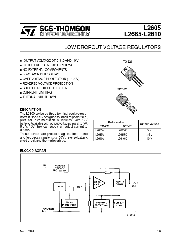
DESCRIPTION
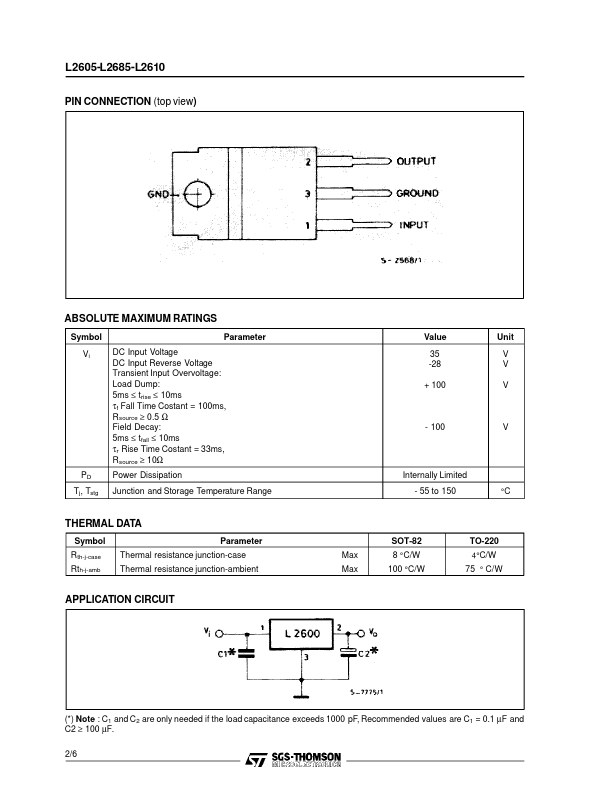
Available with output voltages equal to 5V, 8.5 V, 10V, they can supply an output current to 500mA. BLOCK DIAGRAM Order codes TO-220 L2605V L2685V L2610V SOT-82 L2605X L2685X L2610X Output Voltage 5V 8.5 V 10 V March 1993 1/6 L2605-L2685-L2610 PIN CONNECTION (top view) ABSOLUTE MAXIMUM RATINGS
Symbol Vi Parameter DC Input Voltage DC Input Reverse Voltage Transient Input Overvoltage: Load Dump: 5ms ≤ trise ≤ 10ms τf Fall Time Costant = 100ms, R source ≥ 0.5 Ω Field Decay: 5ms ≤ tfall ≤ 10ms τr Rise Time Costant = 33ms, R source ≥ 10Ω Power Dissipation Junction and Storage Temperature Range Value 35 -28 + 100 Unit V V V - 100 V PD Tj, Tstg Internally Limited - 55 to 150 °C THERMAL DATA Symbol R th-j-case Rth-j-amb Parameter Thermal resistance junction-case Thermal resistance junction-ambient Max Max SOT-82 8 °C/W 100 °C/W TO-220 4°C/W 75 ° C/W APPLICATION CIRCUIT (*) Note : C1 and C 2 are only needed if the load capacitance exceeds 1000 pF, Recommended values are C1 = 0.1 µF and C2 ≥ 100 µF. STMicroelectronics