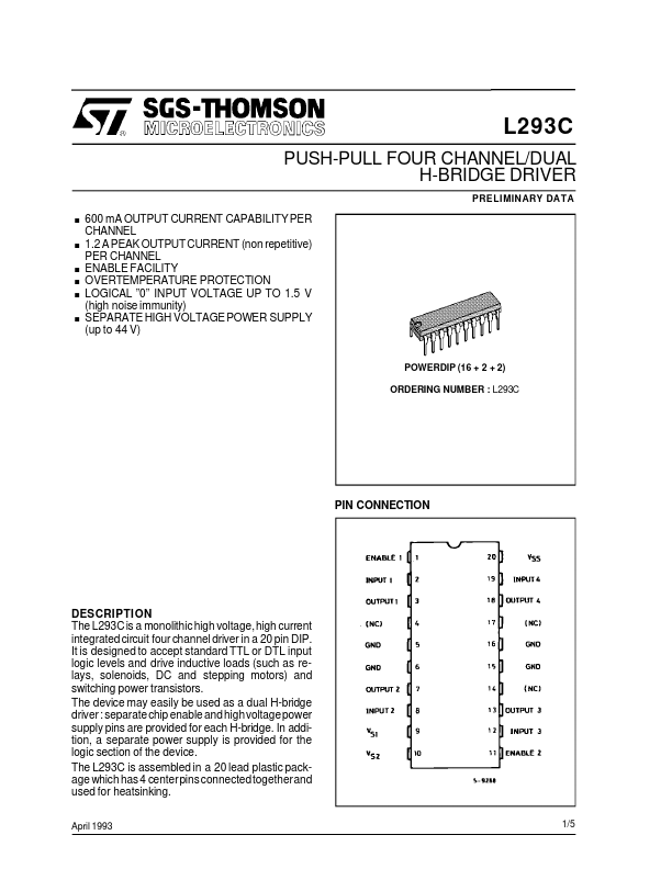
DESCRIPTION
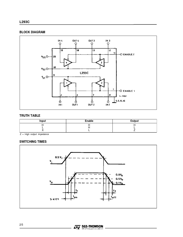
In addition, a separate power supply is provided for the logic section of the device. The L293C is assembled in a 20 lead plastic package which has 4 centerpins connectedtogetherand used for heatsinking. April 1993 1/5 L293C BLOCK DIAGRAM TRUTH TABLE Input H L X Z = High output impedance Enable H H L Output H L Z SWITCHING TIMES 2/5 L293C ABSOLUTE MAXIMUM RATINGS
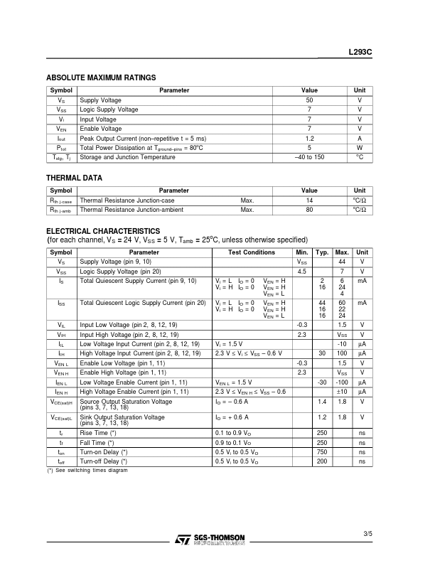
Symbol VS VSS Vi VEN Iout Ptot Tstg, Tj Supply Voltage Logic Supply Voltage Input Voltage Enable Voltage Peak Output Current (non–repetitive t = 5 ms) Total Power Dissipation at Tground–pins = 80 C Storage and Junction Temperature o Parameter Value 50 7 7 7 1.2 5 –40 to 150 Unit V V V V A W o C THERMAL DATA Symbol R th j-case R th j-amb Parameter Thermal Resistance Junction-case Thermal Resistance Junction-ambient Max. Max. Value 14 80 Unit o o C/Ω C/Ω ELECTRICAL CHARACTERISTICS
(for each channel, V S = 24 V, VSS = 5 V, Tamb = 25oC, unless otherwise specified) Symbol VS VSS IS Parameter Supply Voltage (pin 9, 10) L... STMicroelectronics