DESCRIPTION
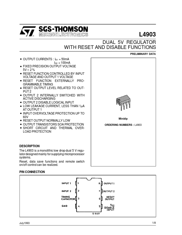
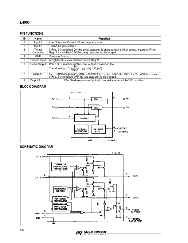
Reset, data save functions and remote switch on/off control can be realized. PIN CONNECTION July1993 1/8 L4903 PIN FUNCTIONS N° 1 2 3 4 5 6 Name Input 1 Input 2 Timing Capacitor GND Disable Input Reset Output Function Low Quiescent Current 50mA Regulator Input 100mA Regulator Input. If Reg. 2 is switched-ON the delay capacitor is charged with a 10µA constant current. When Reg. 2 is switched-OFF the delay capacitor is discharged. Common Ground A high level (> VDT) disables output Reg. 2. When pin 3 reaches 5V the reset output is switched low. 5V ) ; tRD (ms) = Ct (nF). Therefore tRD = C t ( 10µA 5V – 100mA Regulator Output. Enabled if Vo 1 > VRT. DISABLE INPUT < VDT and VIN 2 > VIT. If Reg. 2 is switched-OFF the C02 capacitor is discharged. 5V – 50mA regulator output with low leakage in switch-OFF condition. 7 8 Output 2 Output 1 BLOCK DIAGRAM SCHEMATIC DIAGRAM 2/8 L4903 ABSOLUTE MAXIMUM RATINGS
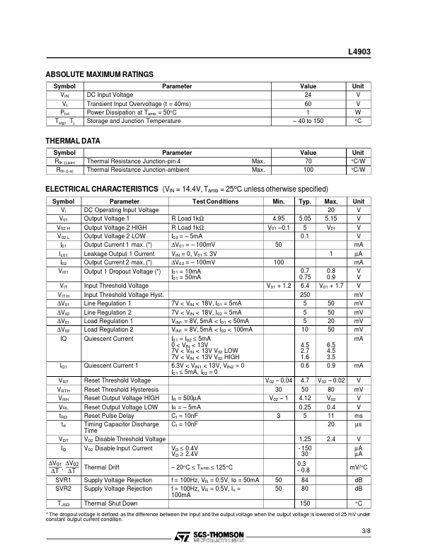
Symbol VIN Vt Ptot Tstg, Tj Parameter DC Input Voltage Transient Input Overvolta... STMicroelectronics