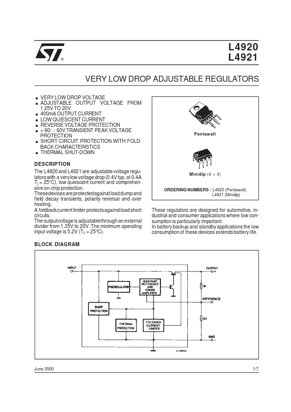
DESCRIPTION
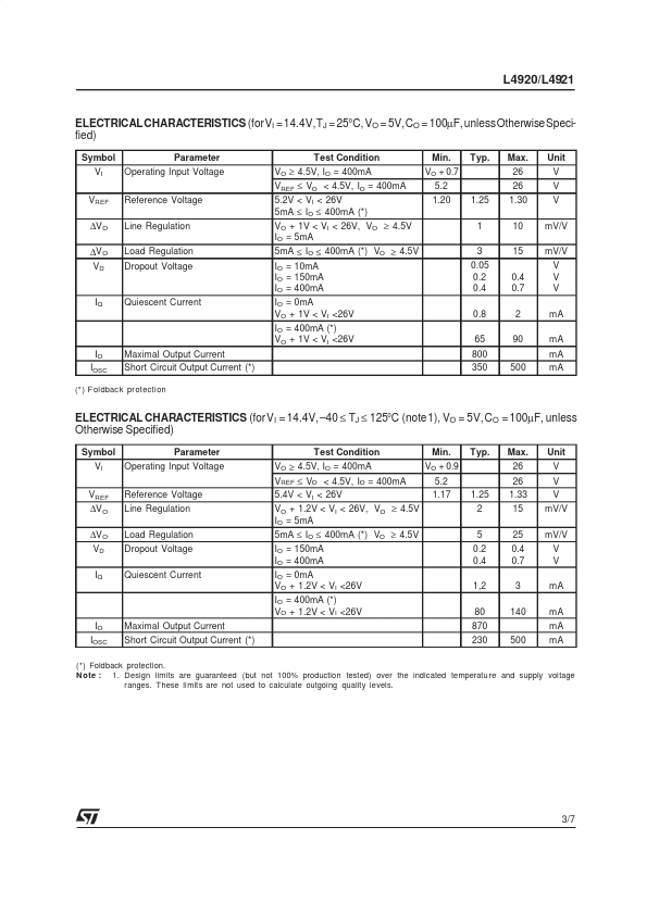
at 0.4A Tj = 25°C), low quiescent current and comprehensive on-chip protection. Thesedevices are protectedagainst load dump and field decay transients, polarity reversal and over heating. A foldbackcurrent limiter protectsagainstload short circuits. The minimum operating input voltage is 5.2V (TJ = 25°C). BLOCK DIAGRAM Minidip (4 + 4) ORDERING NUMBERS : L4920 (Pentawatt) L4921 (Minidip) These regulators are designed for automotive, industrial and consumer applications where low consumption is particularly important. In battery backup and standby applications the low consumption of these devices extends battery life. June 2000 1/7 L4920/L4921 ABSOLUTE MAXIMUM RATINGS
Symbol Vi Parameter DC Input Operating Voltage DC Reverse Input Voltage Transient Input Overvoltages: Load Dump: 5ms ≤ trise ≤ 10ms τf Fall time constant = 100ms R SOURCE ≥ 0.5Ω Field Decay: 5ms ≤ tfall ≤ 10ms, RSOURCE ≥ 10Ω τf Rise time constant = 33ms Value 35 Unit V TJ, TSTG Junction and Storage Temperature Range – 55 to 150 °C PIN CONNECTIONS (top view) TEST AND APPLICATION CIRCUIT C = 100µF is required for stability (ESR ≤ 3Ω over T range) R2 = 6.2KΩ. STMicroelectronics