L4947PD
L4947PD is 5V-0.5A VERY LOW DROP REGULATOR WITH RESET manufactured by STMicroelectronics.
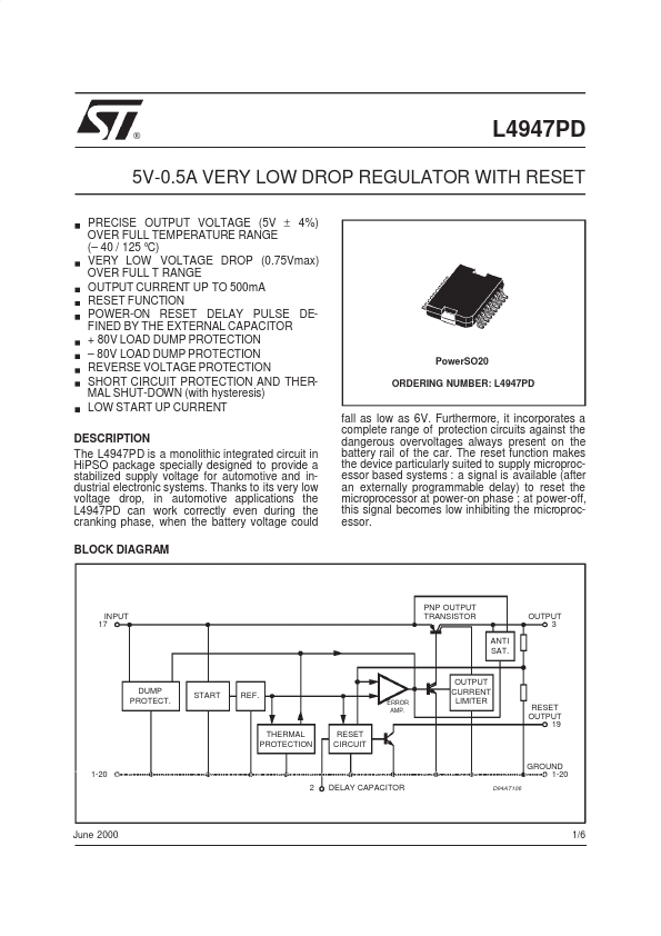
DESCRIPTION
The L4947PD is a monolithic integrated circuit in Hi PSO package specially designed to provide a stabilized supply voltage for automotive and industrial electronic systems. Thanks to its very low voltage drop, in automotive applications the L4947PD can work correctly even during the cranking phase, when the battery voltage could BLOCK DIAGRAM
Power SO20 ORDERING NUMBER: L4947PD fall as low as 6V. Furthermore, it incorporates a plete range of protection circuits against the dangerous overvoltages always present on the battery rail of the car. The reset function makes the device particularly suited to supply microprocessor based systems : a signal is available (after an externally programmable delay) to reset the microprocessor at power-on phase ; at power-off, this signal bees low inhibiting the microprocessor.
INPUT 17
PNP OUTPUT TRANSISTOR ANTI SAT.
OUTPUT 3
DUMP PROTECT.
START
REF.
ERROR AMP.
OUTPUT CURRENT LIMITER
RESET OUTPUT 19
THERMAL PROTECTION
RESET CIRCUIT
GROUND This 1-20 is advanced information on a new product now in development or undergoing evaluation. Details are subject to change without 1-20 notice. 2 DELAY CAPACITOR
D94AT106
June 2000
1/6
ABSOLUTE MAXIMUM RATINGS
Symbol Vi Parameter DC Input Voltage DC Reverse Input Voltage Transient Input Overvoltages : Load Dump : 5ms ≤ trise ≤ 10ms τf Fall Time Constant = 100ms RSOURCE ≥ 0.5Ω Field Decay : 5ms ≤ tfall ≤ 10ms, RSOURCE ≥ 10Ω τr Rise Time Constant = 33ms Low Energy Spike : trise = 1µs, tfall = 500µs, RSOURCE ≥ 10Ω fr Repetition Frequency = 5Hz Reset Output Voltage Junction and Storage Temperature Range Value 35
- 18 80 Unit V V V
- 80 ± 100
VR TJ, Tstg
- 55 to 150
V °C
Note: The circuit is ESD protected according to MIL-STD-883C.
PIN CONNECTION (Top view)
GND DELAY CAP. +VOUT N.C. N.C. N.C. N.C. N.C. N.C. GND 1 2 3 4 5 6 7 8 9 10
D94AT107A
20 19 18 17 16 15 14 13 12 11
GND RESET N.C. +VIN N.C. N.C. N.C. N.C. N.C. GND
THERMAL DATA
Symbol R th...