DESCRIPTION
FEATURES
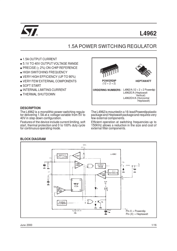
of the device include current limiting, soft start, thermal protection and 0 to 100% duty cycle for continuous operating mode. Efficient operation at switching frequencies up to 150KHz allows a reduction in the size and cost of external filter components. BLOCK DIAGRAM Pin X = Powerdip Pin (X) = Heptawatt June 2000 1/16 L4962 ABSOLUTE MAXIMUM RATINGS
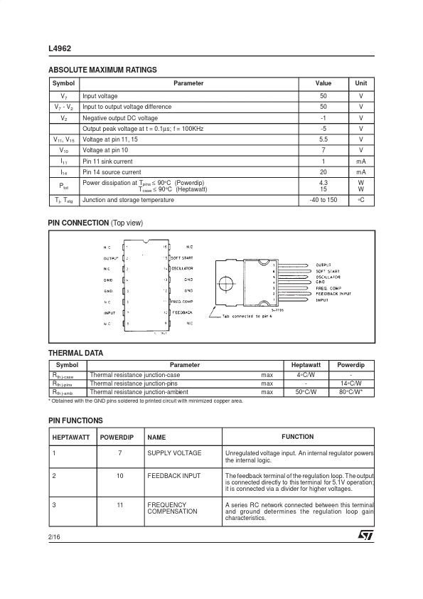
Symbol V7 V7 - V 2 V2 Input voltage Input to output voltage difference Negative output DC voltage Output peak voltage at t = 0.1µs; f = 100KHz V11, V15 V10 I11 I14 Ptot Tj, Tstg Voltage at pin 11, 15 Voltage at pin 10 Pin 11 sink current Pin 14 source current Power dissipation at Tpins ≤ 90°C (Powerdip) Tcase ≤ 90°C (Heptawatt) Junction and storage temperature Parameter Value 50 50 -1 -5 5.5 7 1 20 4.3 15 -40 to 150 Unit V V V V V V mA mA W W °C PIN CONNECTION (Top view) THERMAL DATA Symbol R th j-case R th j-pins R th j-amb Parameter Thermal resistance junction-case Thermal resistance junction-pins Thermal resistance... STMicroelectronics