DESCRIPTION
FEATURES
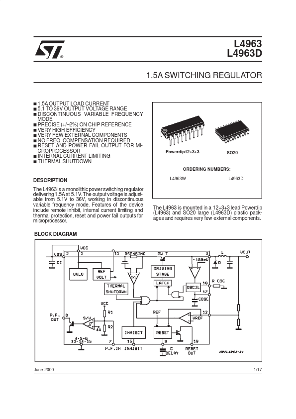
of the device include remote inhibit, internal current limiting and thermal protection, reset and power fail outputs for microprocessor. BLOCK DIAGRAM L4963W L4963D The L4963 is mounted in a 12+3+3 lead Powerdip (L4963) and SO20 large (L4963D) plastic packages and requires very few external components. June 2000 This is advanced information on a new product now in development or underogin evaluation. Details are subject to change without notice. 1/17 L4963 - L4963D ABSOLUTE MAXIMUM RATINGS
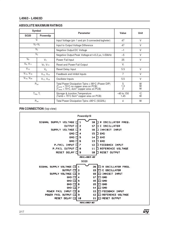
Symbol SO20 Vi V3–V2 V2 V2 V8 V9, V11 V 10 V13 , V18 V19 , V20 Ptot V7 V8, V10 V9 V12, V16 V17, V18 Powerdip Input Voltage (pin 1 and pin 3 connected togheter) Input to Output Voltage Difference Negative Output DC Voltage Negative Output Peak Voltage at t=0.2 µs, f=50kHz Power Fail Input Reset and Power Fail Output Reset Delay Input Feedback and Inhibit Inputs Oscillator Inputs Total Power Dissipation Tpins ≤ 90°C (Power DIP) (Tamb = 70°C no copper area on PCB) 2 (Tamb = 70°C, 4c... STMicroelectronics