STMicroelectronics LF151
The devices feature high slew rates, low input bias and offset currents, and low offset voltage temperature coefficient. The magnitude of the input voltage must never exceed the magnitude of the supply voltage or 15 volts, whichever is less.| Part No. | LF151 |
|---|---|
| Datasheet | LF151 Download |
| Manufacturer |  STMicroelectronics |
| Description | WIDE BANDWIDTH SINGLE J-FET OPERATIONAL AMPLIFIER |
| Buy | Stock & Price |
DESCRIPTION
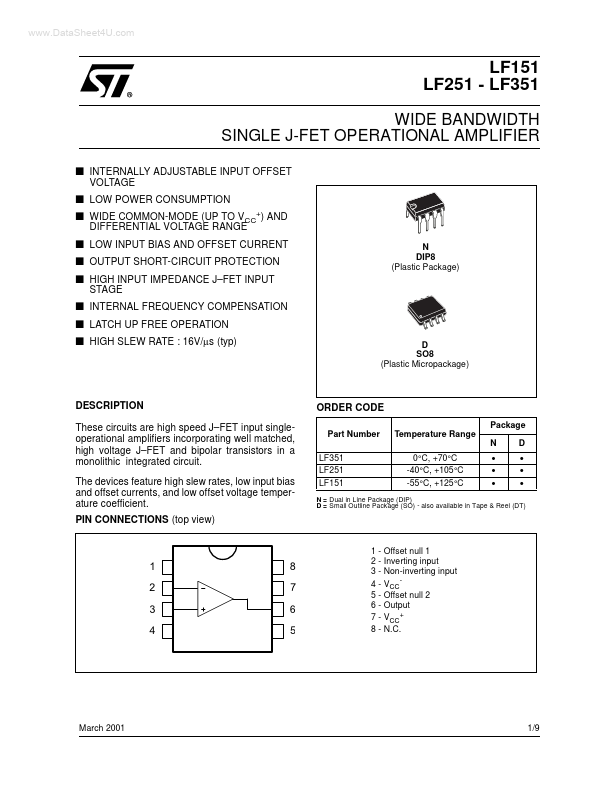
These circuits are high speed J–FET input singleoperational amplifiers incorporating well matched, high voltage J–FET and bipolar transistors in a monolithic integrated circuit. PIN CONNECTIONS (top view) ORDER CODE Package Part Number LF351 LF251 LF151 Temperature Range N 0°C, +70°C -40°C, +105°C -55°C, +125°C●
●
● D
●
●
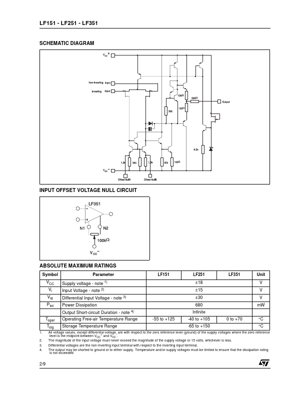
● N = Dual in Line Package (DIP) D = Small Outline Package (SO) - also available in Tape & Reel (DT) 1 2 3 4 8 7 6 5 12345678- Offset null 1 Inverting input Non-inverting input VCCOffset null 2 Output VCC+ N.C. March 2001 1/9 LF151 - LF251 - LF351 SCHEMATIC DIAGRAM INPUT OFFSET VOLTAGE NULL CIRCUIT
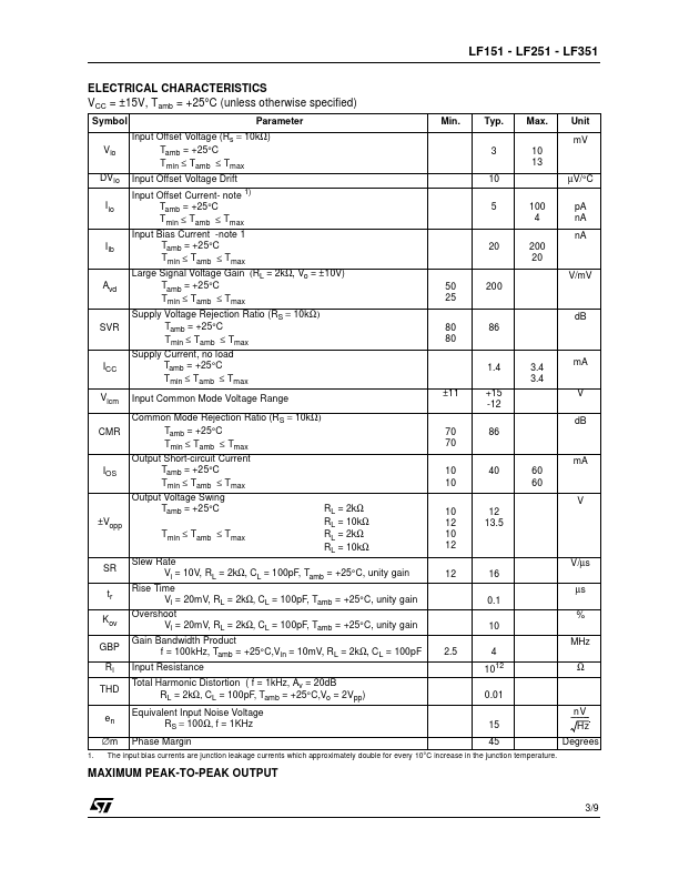
ABSOLUTE MAXIMUM RATINGS
Symbol VCC Vi Vid Ptot Toper Tstg 1. 2. 3. 4. Parameter Supply voltage - note Input Voltage - note Power Dissipation Output Short-circuit Duration - note Storage Temperature Range 4) 2) 1) LF151 LF251 LF351 Unit V V V mW ±18 ±15 ±30 680 Infinite -55 to +125 -40 to +105 -65 to +150 0 to +70 Differential Input Voltage - note 3) Operating...