DESCRIPTION
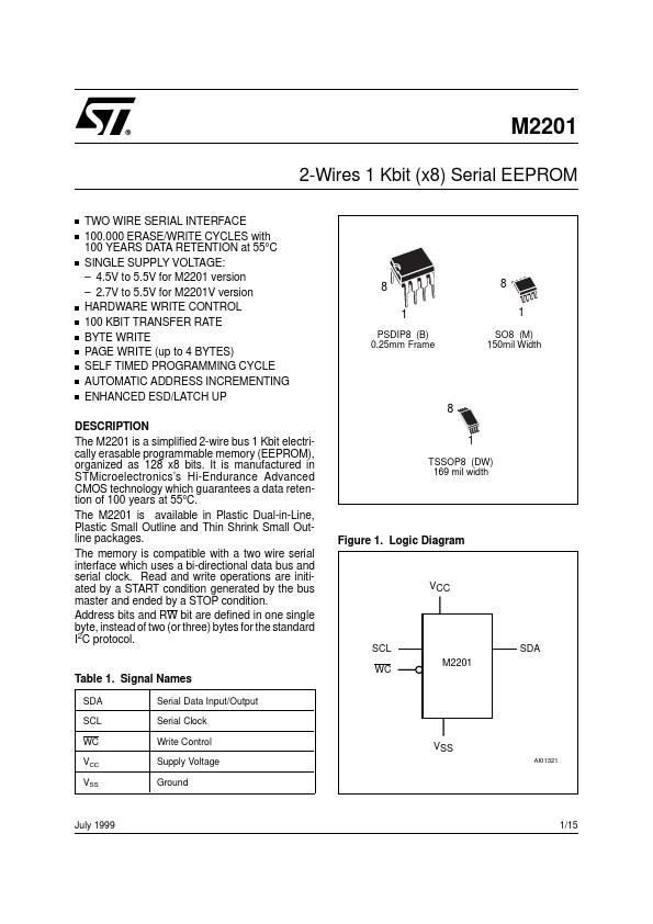
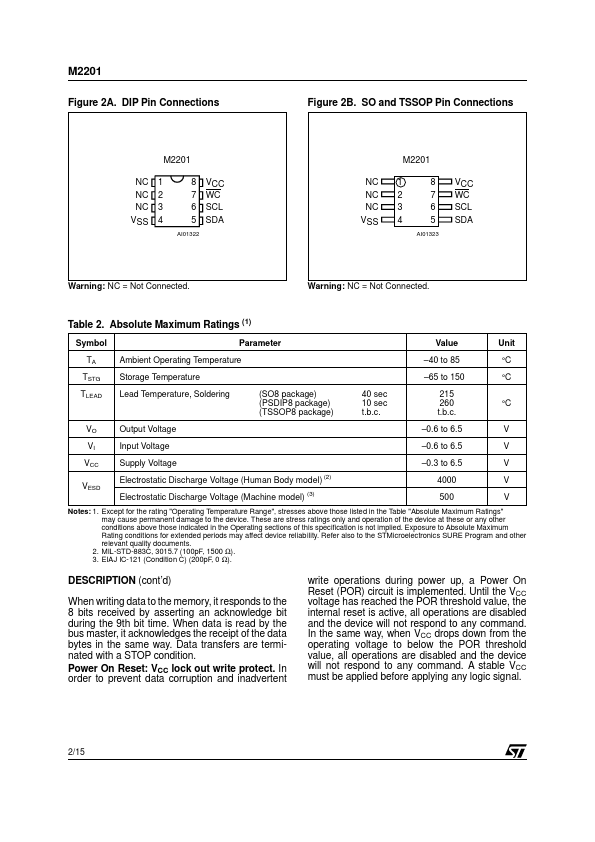
The memory is compatible with a two wire serial interface which uses a bi-directional data bus and serial clock. Read and write operations are initiated by a START condition generated by the bus master and ended by a STOP condition. Address bits and RW bit are defined in one single byte, instead of two (or three) bytes for the standard I2C protocol. 8 1 PSDIP8 (B) 0.25mm Frame 8 1 SO8 (M) 150mil Width 8 1 TSSOP8 (DW) 169 mil width Figure 1. Logic Diagram VCC SCL WC M2201 SDA Table 1. Signal Names SDA SCL WC VCC VSS Serial Data Input/Output Serial Clock Write Control Supply Voltage Ground VSS AI01321 July 1999 1/15 M2201 Figure 2A. DIP Pin Connections Figure 2B. SO and TSSOP Pin Connections M2201 NC NC NC VSS 1 2 3 4 8 7 6 5 AI01322 M2201 VCC WC SCL SDA NC NC NC VSS 1 2 3 4 8 7 6 5 AI01323 VCC WC SCL SDA Warning: NC = Not Connected. Warning: NC = Not Connected. Table 2. ABSOLUTE MAXIMUM RATINGS
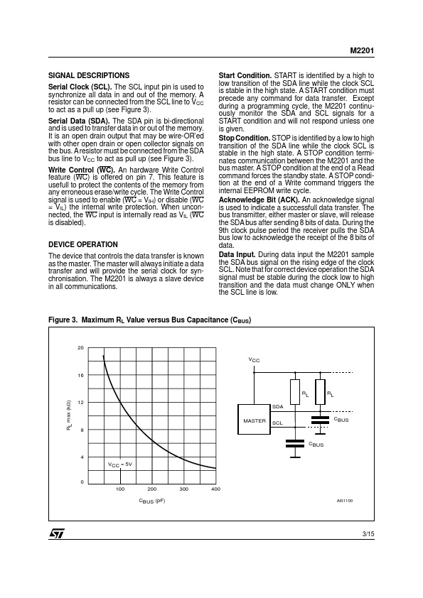
(1) Symbol TA TSTG TLEAD Parameter Ambient Operating Temperature Storage Temperature Lead Temperature, Soldering (SO8 package) (PSDIP8 package) (TSSOP8 package) 40 sec 10 sec t.b.c. STMicroelectronics