DESCRIPTION
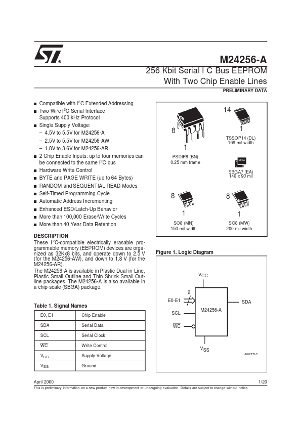
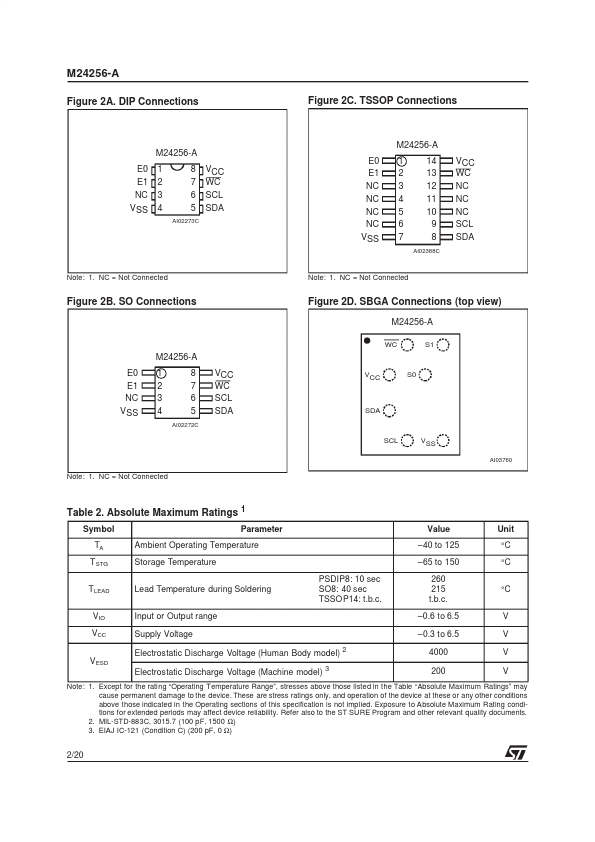
These I 2C-compatible electrically erasable programmable memory (EEPROM) devices are organized as 32Kx8 bits, and operate down to 2.5 V (for the M24256-AW), and down to 1.8 V (for the M24256-AR). Figure 1. Logic Diagram VCC 2 E0-E1 Table 1. Signal Names E0, E1 SDA SCL WC VCC VSS Chip Enable Serial Data Serial Clock Write Control Supply Voltage Ground SDA M24256-A SCL WC VSS AI02271C April 2000 This is preliminary information on a new product now in development or undergoing evaluation. Details are subject to change without notice. 1/20 M24256-A Figure 2A. DIP Connections Figure 2C. TSSOP Connections M24256-A M24256-A E0 E1 NC VSS 1 2 3 4 8 7 6 5 AI02273C VCC WC SCL SDA E0 E1 NC NC NC NC VSS 1 2 3 4 5 6 7 14 13 12 11 10 9 8 AI02388C VCC WC NC NC NC SCL SDA Note: 1. NC = Not Connected Note: 1. NC = Not Connected Figure 2B. SO Connections Figure 2D. SBGA Connections (top view) M24256-A WC S1 M24256-A E0 E1 NC VSS 1 2 3 4 8 7 6 5 AI02272C VCC WC SCL SDA VCC S0 SDA SCL VSS AI03760 Note: 1. STMicroelectronics