M24M01-V
M24M01-V is 1 Mbit Serial IC Bus EEPROM manufactured by STMicroelectronics.
M24M01
1 Mbit Serial I²C Bus EEPROM
Features
SUMMARY 2 s 400 kHz High Speed Two Wire I C Serial Interface s
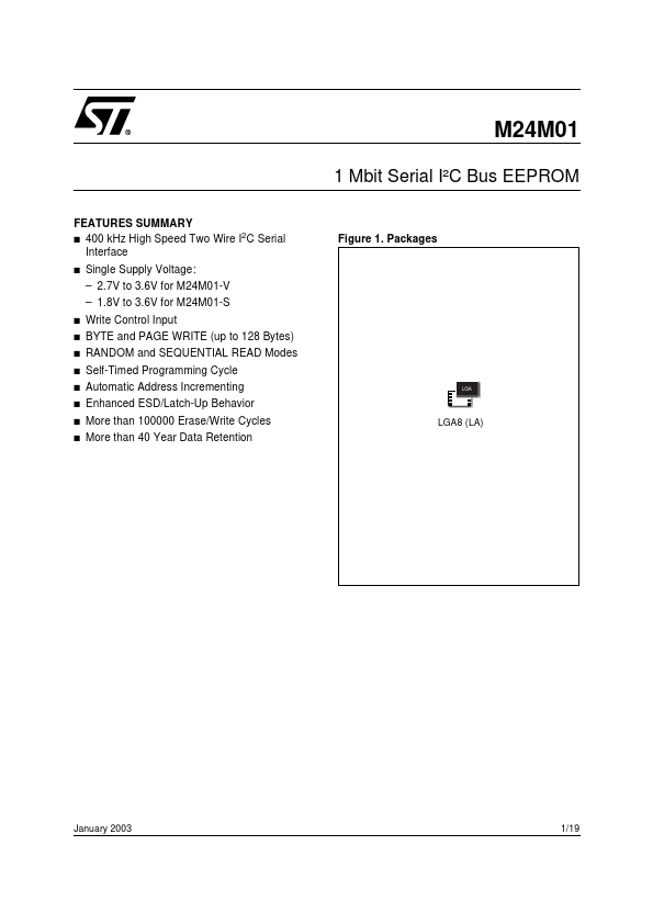
Figure 1. Packages
Single Supply Voltage:
- 2.7V to 3.6V for M24M01-V
- 1.8V to 3.6V for M24M01-S s s s s s s s s
Write Control Input BYTE and PAGE WRITE (up to 128 Bytes) RANDOM and SEQUENTIAL READ Modes Self-Timed Programming Cycle Automatic Address Incrementing Enhanced ESD/Latch-Up Behavior More than 100000 Erase/Write Cycles More than 40 Year Data Retention
LGA8 (LA)
January 2003
1/19
M24M01
SUMMARY DESCRIPTION The M24M01 is a 1 Mbit (131,072 x 8) electrically erasable programmable memory (EEPROM) accessed by an I2C-patible bus. Figure 2. Logic Diagram
When...