DESCRIPTION
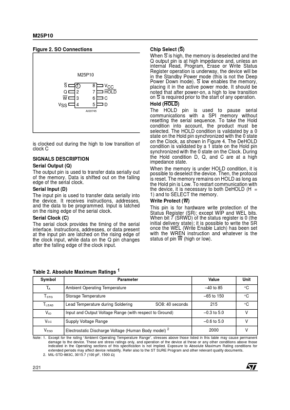
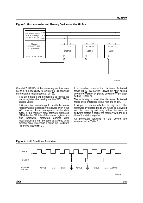
The device connected to the bus is selected when the chip select input (S) goes low. Data is clocked in during the low to high transition of clock C, data Figure 1. Logic Diagram VCC Table 1. Signal Names C D Q Serial Clock Serial Data Input Serial Data Output Chip Select D C S W HOLD M25P10 Q S W HOLD VCC VSS Write Protect Hold Supply Voltage Ground VSS AI03744 June 2000 This is preliminary information on a new product now in development or undergoing evaluation. Details are subject to change without notice. 1/21 M25P10 Figure 2. SO Connections Chip Select (S) When S is high, the memory is deselected and the Q output pin is at high impedance and, unless an internal Read, Program, Erase or Write Status Register operation is underway, the device will be in the Standby Power mode (this is not the Deep Power Down mode). S low enables the memory, placing it in the active power mode. It should be noted that after power-on, a high to low transition on S is required prior to the start of any operation. STMicroelectronics