M25P40 Overview
Key Specifications
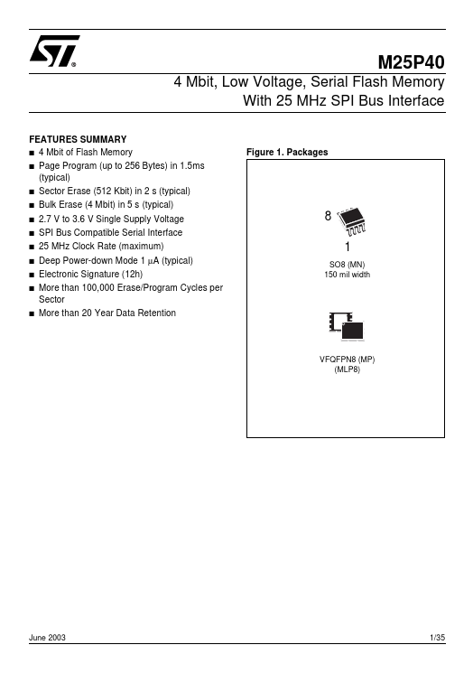
Package: SOP
Pins: 8
Operating Voltage: 2.7 V
Max Voltage (typical range): 3.6 V
Key Features
- Logic Diagram VCC Figure
- SO and VFQFPN Connections M25P40 S Q W VSS 1 2 3 4 8 7 6 5 AI04091B VCC HOLD C D D C S W HOLD M25P40 Q Note
- See page 31 (onwards) for package dimensions, and how to identify pin-1. VSS AI04090 Table