FEATURES
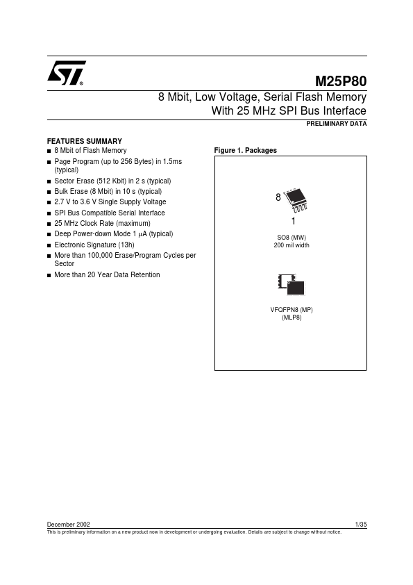
SUMMARY s 8 Mbit of Flash Memory s Figure 1. Packages Page Program (up to 256 Bytes) in 1.5ms (typical) Sector Erase (512 Kbit) in 2 s (typical) Bulk Erase (8 Mbit) in 10 s (typical) 2.7 V to 3.6 V Single Supply Voltage SPI Bus Compatible Serial Interface 25 MHz Clock Rate (maximum) Deep Power-down Mode 1 µA (typical) Electronic Signature (13h) More than 100,000 Erase/Program Cycles per Sector More than 20 Year Data Retention s s s s s s s s 8 1 SO8 (MW) 200 mil width s VFQFPN8 (MP) (MLP8) December 2002 This is preliminary information on a new product now in development or undergoing evaluation. Details are subject to change without notice. 1/35 M25P80 SUMMARY DESCRIPTION
Each page is 256 bytes wide. Thus, the whole memory can be viewed as consisting of 4096 pages, or 1,048,576 bytes. The whole memory can be erased using the Bulk Erase instruction, or a sector at a time, using the Sector Erase instruction. Figure 2. Logic Diagram VCC Figure 3. SO and VFQFPN Connections M25P80 S Q W VSS 1 2 3 4 8 7 6 5 AI04965B VCC HOLD C D D C S W HOLD M25P80 Q Note: 1. STMicroelectronics