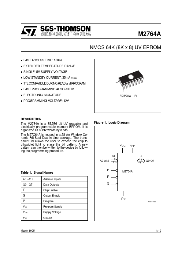
DESCRIPTION
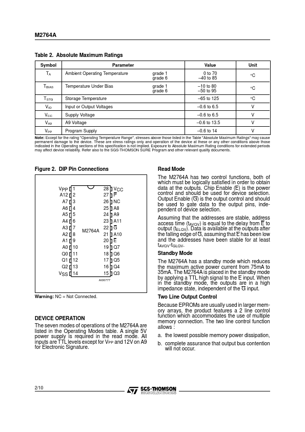
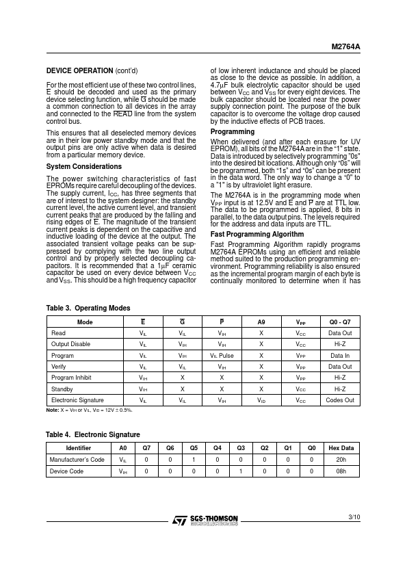
It is organized as 8,192 words by 8 bits. The transparent lid allows the user to expose the chip to ultraviolet light to erase the bit pattern. A new pattern can then be written to the device by following the programming procedure. Figure 1. Logic Diagram VCC VPP 13 A0-A12 8 Q0-Q7 Table 1. Signal Names A0 - A12 Q0 - Q7 E G P VPP VCC VSS Address Inputs Data Outputs Chip Enable Output Enable Program Program Supply Supply Voltage Ground P E G M2764A VSS AI00776B March 1995 1/10 M2764A Table 2. ABSOLUTE MAXIMUM RATINGS
Symbol TA TBIAS TSTG VIO VCC VA9 VPP Parameter Ambient Operating Temperature Temperature Under Bias Storage Temperature Input or Output Voltages Supply Voltage A9 Voltage Program Supply grade 1 grade 6 grade 1 grade 6 Value 0 to 70 –40 to 85 –10 to 80 –50 to 95 –65 to 125 –0.6 to 6.5 –0.6 to 6.5 –0.6 to 13.5 –0.6 to 14 Unit °C °C °C V V V V Note: Except for the rating "Operating Temperature Range", stresses above those listed in the Table "ABSOLUTE MAXIMUM RATINGS
" may cause permanent damage to the device. STMicroelectronics