DESCRIPTION
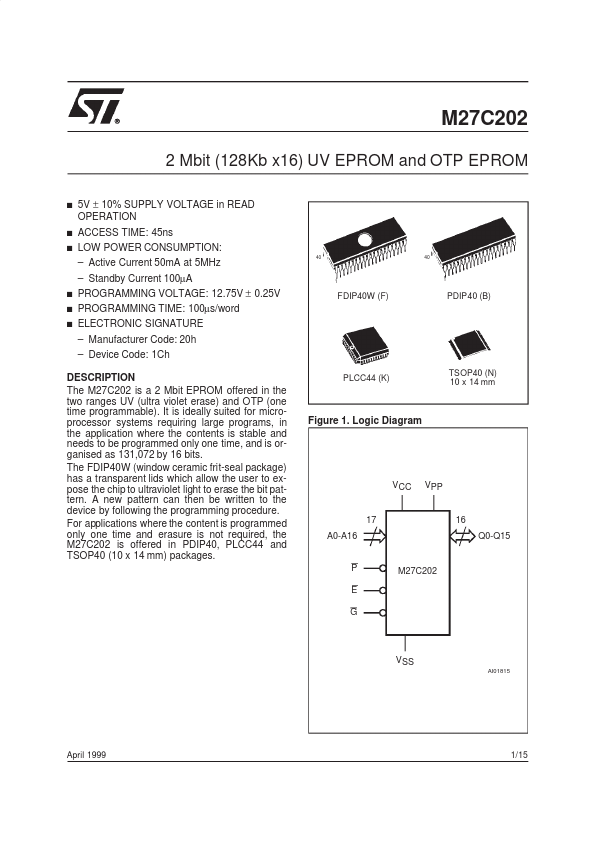
A new pattern can then be written to the device by following the programming procedure. For applications where the content is programmed only one time and erasure is not required, the M27C202 is offered in PDIP40, PLCC44 and TSOP40 (10 x 14 mm) packages. PLCC44 (K) TSOP40 (N) 10 x 14 mm Figure 1. Logic Diagram VCC VPP 17 A0-A16 16 Q0-Q15 P E G M27C202 VSS AI01815 April 1999 1/15 M27C202 Figure 2A. DIP Connections Figure 2B. TSOP Connections VPP E Q15 Q14 Q13 Q12 Q11 Q10 Q9 Q8 VSS Q7 Q6 Q5 Q4 Q3 Q2 Q1 Q0 G 40 1 39 2 38 3 37 4 36 5 35 6 34 7 33 8 32 9 31 10 M27C202 30 11 29 12 28 13 27 14 26 15 25 16 17 24 18 23 19 22 20 21 AI02784 VCC P A16 A15 A14 A13 A12 A11 A10 A9 VSS A8 A7 A6 A5 A4 A3 A2 A1 A0 A9 A10 A11 A12 A13 A14 A15 A16 P VCC VPP E DQ15 DQ14 DQ13 DQ12 DQ11 DQ10 DQ9 DQ8 1 40 10 11 M27C202 31 30 20 21 AI01817B VSS A8 A7 A6 A5 A4 A3 A2 A1 A0 G DQ0 DQ1 DQ2 DQ3 DQ4 DQ5 DQ6 DQ7 VSS Figure 2C. LCC Connections Table 1. Signal Names A0-A16 Q0-Q15 Address Inputs Data Outputs C... STMicroelectronics