M27V256
M27V256 is 256 Kbit 32Kb x 8 Low Voltage UV EPROM and OTP EPROM manufactured by STMicroelectronics.
The M27V256 is a low voltage 256 Kbit EPROM offered in the two ranges UV (ultra violet erase) and OTP (one time programmable). It is ideally suited for microprocessor systems and is organized as 32,768 by 8 bits. The M27V256 operates in the read mode with a supply voltage as low as 3V. The decrease in operating power allows either a reduction of the size of the battery or an increase in the time between battery recharges. The FDIP28W (window ceramic frit-seal package) has a transparent lid which allows the user to expose the chip to ultraviolet light to erase the bit pattern. A new pattern can then be written to the device by following the programming procedure.
PLCC32 (K)
TSOP28 (N) 8 x 13.4mm
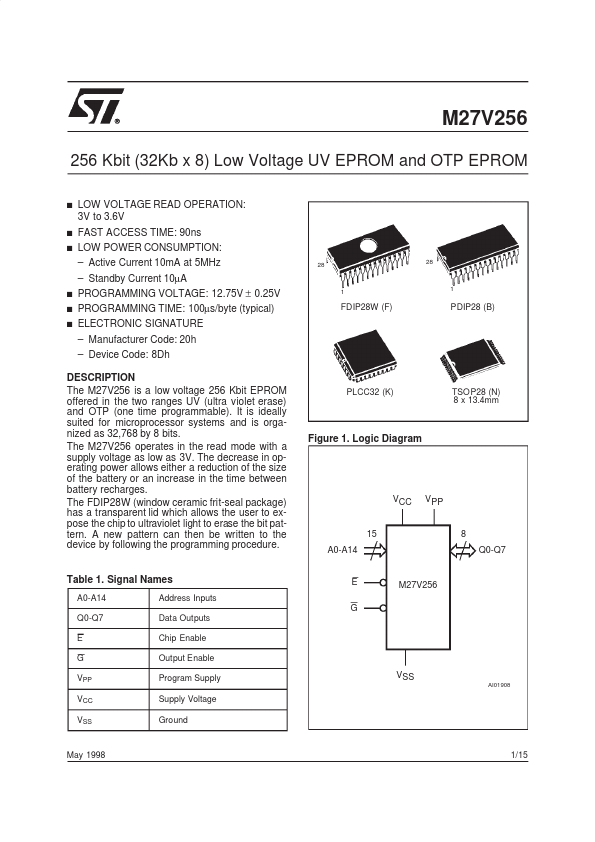
Figure 1. Logic Diagram
15 A0-A14
8 Q0-Q7
Table 1. Signal Names
A0-A14 Q0-Q7 E G VPP VCC VSS Address Inputs
Data Outputs Chip Enable Output Enable Program Supply Supply Voltage Ground
AI01908
May 1998
1/15
Figure 2A. DIP Pin Connections Figure 2B. LCC Pin Connections
AI01909
VSS DU Q3 Q4 Q5
AI01910
Warning: NC = Not Connected, DU = Dont’t Use.
Figure 2C. TSOP Pin Connections
For applications where the content is programmed only one time and erasure is not required, the M27V256 is offered in PDIP28, PLCC32 and TSOP28 (8 x 13.4 mm) packages.
A10 E Q7 Q6 Q5 Q4 Q3 VSS Q2 Q1 Q0 A0 A1 A2
G A11 A9 A8 A13 A14 VCC VPP A12 A7 A6 A5 A4 A3
28 1
15 14
AI01911
DEVICE OPERATION The modes of operation of the M27V256 are listed in the Operating Modes. A single power supply is required in the read mode. All inputs are TTL levels except for VPP and 12V on A9 for Electronic Signature. Read Mode The M27V256 has two control functions, both of which must be logically active in order to obtain data at the outputs. Chip Enable (E) is the power control and should be used for device selection. Output Enable (G) is the output control and should be used to gate data to the output pins, independent of device selection....