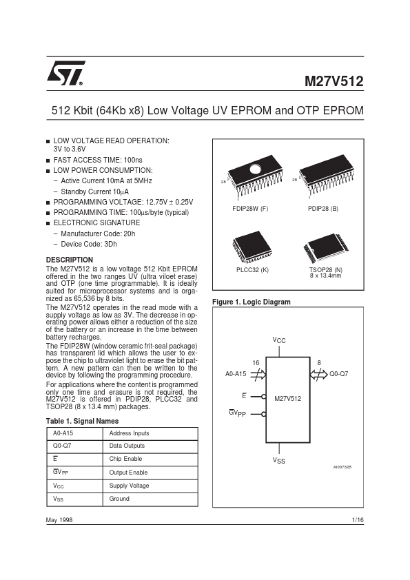
DESCRIPTION
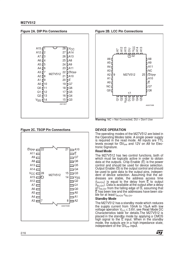
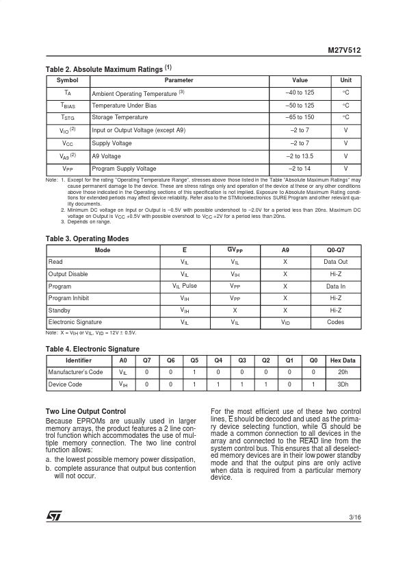
The decrease in operating power allows either a reduction of the size of the battery or an increase in the time between battery recharges. The FDIP28W (window ceramic frit-seal package) has transparent lid which allows the user to expose the chip to ultraviolet light to erase the bit pattern. A new pattern can then be written to the device by following the programming procedure. For applications where the content is programmed only one time and erasure is not required, the M27V512 is offered in PDIP28, PLCC32 and TSOP28 (8 x 13.4 mm) packages. Table 1. Signal Names A0-A15 Q0-Q7 E GV PP VCC VSS Address Inputs Data Outputs Chip Enable Output Enable Supply Voltage Ground PLCC32 (K) TSOP28 (N) 8 x 13.4mm Figure 1. Logic Diagram VCC 16 A0-A15 8 Q0-Q7 E GVPP M27V512 VSS AI00732B May 1998 1/16 M27V512 Figure 2A. DIP Pin Connections Figure 2B. LCC Pin Connections AI01907 VSS DU Q3 Q4 Q5 AI00733B A15 A12 A7 A6 A5 A4 A3 A2 A1 A0 Q0 Q1 Q2 VSS 1 28 2 27 3 26 4 25 5 24 6 23 7 22 M27V512... STMicroelectronics