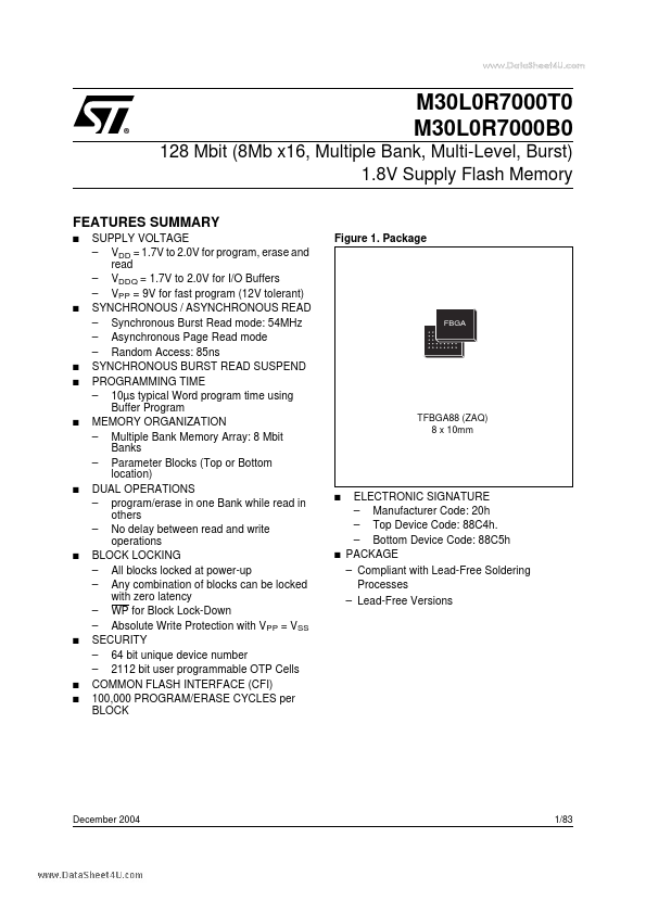
M30L0R7000B0 Description
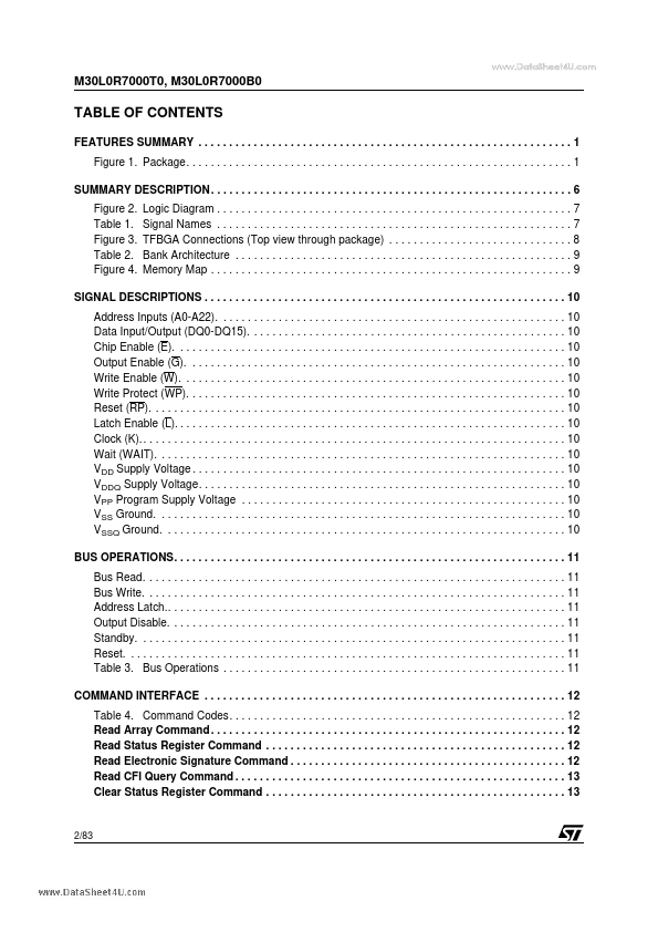
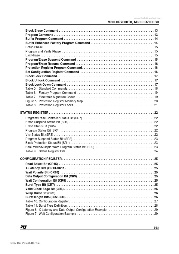
7 TFBGA Connections (Top view through package) . 10 Address Inputs (A0-A22). 10 Data Input/Output (DQ0-DQ15).
M30L0R7000B0 Key Features
- VDD = 1.7V to 2.0V for program, erase and read
- VDDQ = 1.7V to 2.0V for I/O Buffers
- VPP = 9V for fast program (12V tolerant) SYNCHRONOUS / ASYNCHRONOUS READ
- Synchronous Burst Read mode: 54MHz
- Asynchronous Page Read mode
- Random Access: 85ns SYNCHRONOUS BURST READ SUSPEND PROGRAMMING TIME
- 10µs typical Word program time using Buffer Program MEMORY ORGANIZATION
- Multiple Bank Memory Array: 8 Mbit Banks
- Parameter Blocks (Top or Bottom location) DUAL OPERATIONS
- program/erase in one Bank while read in others


