DESCRIPTION
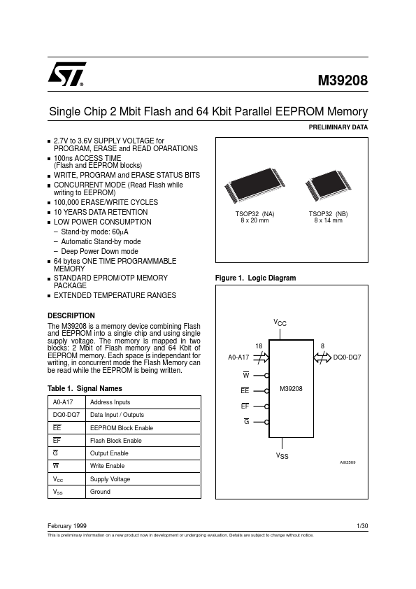
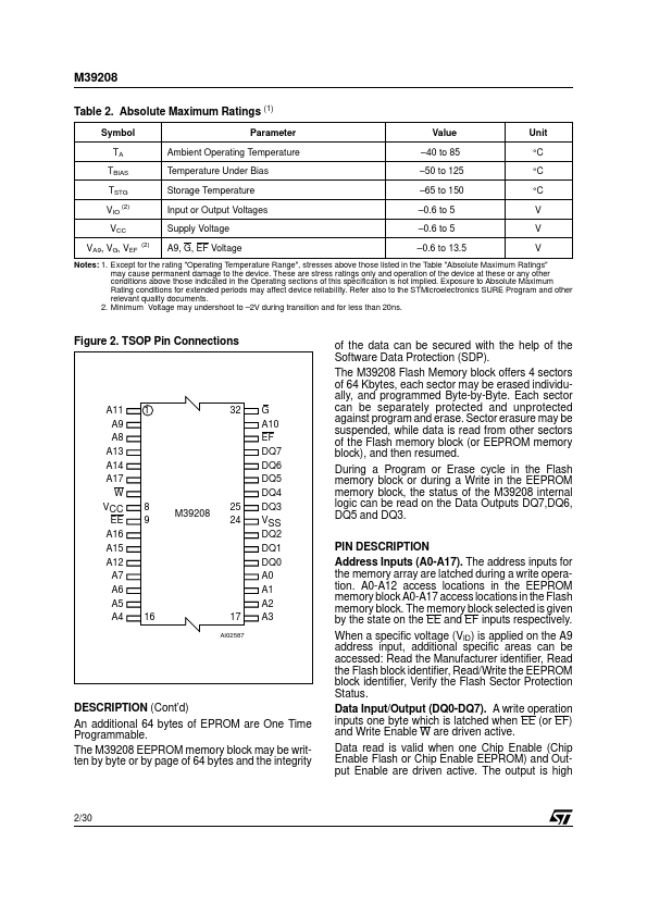
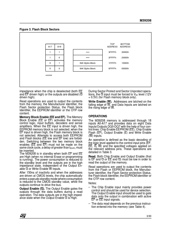
Table 1. Signal Names A0-A17 DQ0-DQ7 EE EF G W VCC VSS Address Inputs Data Input / Outputs TSOP32 (NA) 8 x 20 mm TSOP32 (NB) 8 x 14 mm Figure 1. Logic Diagram VCC 18 A0-A17 W EE EF G M39208 8 DQ0-DQ7 EEPROM Block Enable Flash Block Enable Output Enable Write Enable Supply Voltage Ground VSS AI02589 February 1999 This is preliminary information on a new product now in development or undergoing evaluation. Details are subject to change without notice. 1/30 M39208 Table 2. ABSOLUTE MAXIMUM RATINGS
(1) Symbol TA TBIAS TSTG VIO (2) VCC VA9, VG, VEF (2) Parameter Ambient Operating Temperature Temperature Under Bias Storage Temperature Input or Output Voltages Supply Voltage A9, G, EF Voltage Value –40 to 85 –50 to 125 –65 to 150 –0.6 to 5 –0.6 to 5 –0.6 to 13.5 Unit °C °C °C V V V Notes: 1. Except for the rating "Operating Temperature Range", stresses above those listed in the Table "ABSOLUTE MAXIMUM RATINGS
" may cause permanent damage to the device. These are stress ratings only and operation of the device at these or any other conditions above those indicated in the Operating sections of this specification is not implied. STMicroelectronics