STMicroelectronics M50FLW080A
8 Mbit (13 x 64KByte Blocks 3 x 16 x 4KByte Sectors) 3V Supply Firmware Hub / Low Pin Count Flash Memory
| Part No. | M50FLW080A |
|---|---|
| Datasheet | M50FLW080A Download |
| Manufacturer |  STMicroelectronics |
| Description | 8 Mbit (13 x 64KByte Blocks 3 x 16 x 4KByte Sectors) 3V Supply Firmware Hub / Low Pin Count Flash Memory |
| Buy | Stock & Price |
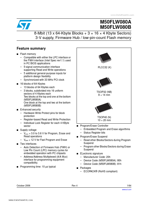
M50FLW080A M50FLW080B 8-Mbit (13 x 64-Kbyte Blocks + 3 × 16 × 4 Kbyte Sectors) 3-V supply, Firmware Hub / low-pin-count Flash memory Feature summary
● Flash memory – Compatible with either the LPC interface or the FWH interface (Intel Spec rev1.1) used in PC BIOS applications – 5-signal communication interface supporting Read and Write operations – 5 additional general-purpose inputs for platform design flexibility – Synchronized with 33 MHz PCI clock 16 blocks of 64 Kbytes – 13 blocks of 64 Kbytes each – 3 blocks, subdivided into 16 uniform sectors of 4 Kbytes each Two blocks at the top and one at the bottom (M50FLW080A) One block at the top and two at the bottom (M50FLW080B) Enhanced security – Hardware Write Protect pins for block protection – Register-based Read and Write Protection – Individual Lock Register for each 4 KByte sector Supply voltage – VCC = 3.0 to 3.6 V for Program, Erase and Read operations – VPP = 12 V for Fast Program and Erase Two interfaces – Auto Detection of F...
● Flash memory – Compatible with either the LPC interface or the FWH interface (Intel Spec rev1.1) used in PC BIOS applications – 5-signal communication interface supporting Read and Write operations – 5 additional general-purpose inputs for platform design flexibility – Synchronized with 33 MHz PCI clock 16 blocks of 64 Kbytes – 13 blocks of 64 Kbytes each – 3 blocks, subdivided into 16 uniform sectors of 4 Kbytes each Two blocks at the top and one at the bottom (M50FLW080A) One block at the top and two at the bottom (M50FLW080B) Enhanced security – Hardware Write Protect pins for block protection – Register-based Read and Write Protection – Individual Lock Register for each 4 KByte sector Supply voltage – VCC = 3.0 to 3.6 V for Program, Erase and Read operations – VPP = 12 V for Fast Program and Erase Two interfaces – Auto Detection of F...