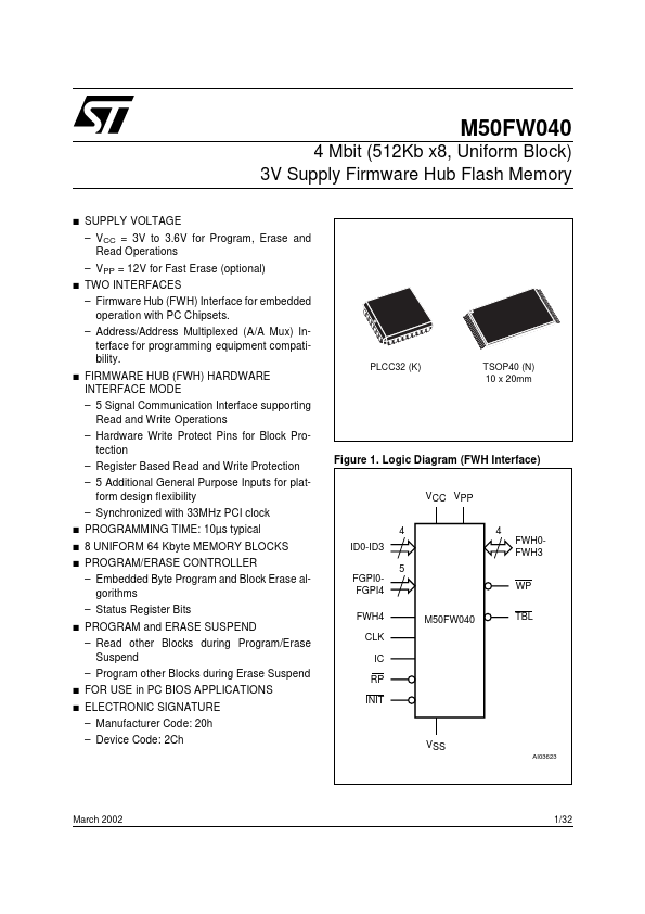
APPLICATIONS
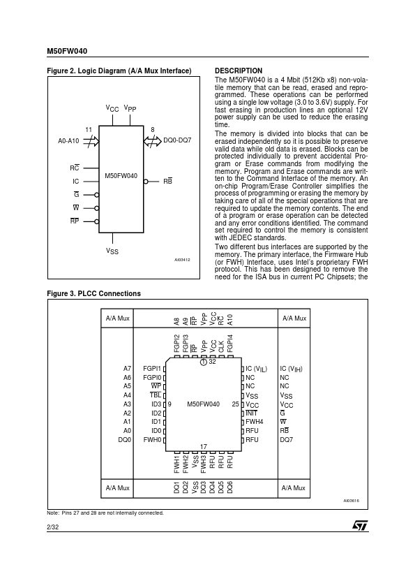
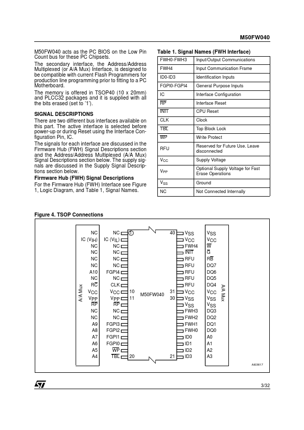
ELECTRONIC SIGNATURE – Manufacturer Code: 20h – Device Code: 2Ch VSS AI03623 March 2002 1/32 M50FW040 Figure 2. Logic Diagram (A/A Mux Interface) DESCRIPTION
The memory is divided into blocks that can be erased independently so it is possible to preserve valid data while old data is erased. Blocks can be protected individually to prevent accidental Program or Erase commands from modifying the memory. Program and Erase commands are written to the Command Interface of the memory. An on-chip Program/Erase Controller simplifies the process of programming or erasing the memory by taking care of all of the special operations that are required to update the memory contents. The end of a program or erase operation can be detected and any error conditions identified. The command set required to control the memory is consistent with JEDEC standards. Two different bus interfaces are supported by the memory. The primary interface, the Firmware Hub (or FWH) Interface, uses Intel’s proprietary FWH protocol. STMicroelectronics