DESCRIPTION
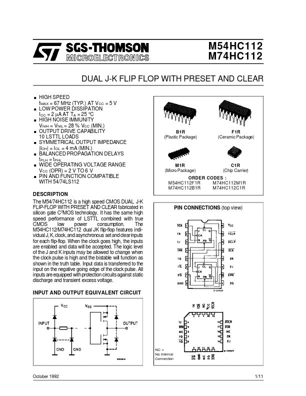
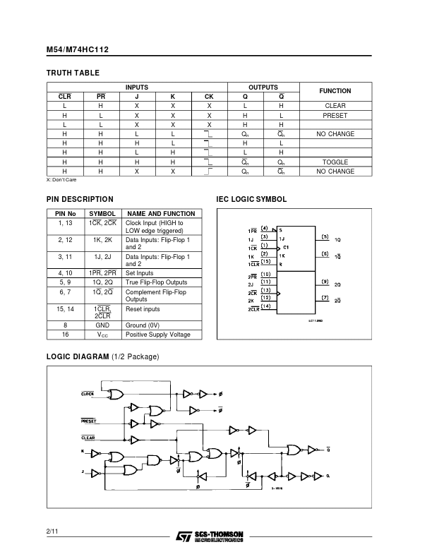
When the clock goes high, the inputs are enabled and data will be accepted. The logic level of the J and K inputs may be allowed to change when the clock pulse is high and the bistable will function as shown in the truth table. Input data is transferred to the input on the negative going edge of the clock pulse. All inputs are equipped withprotection circuits against static discharge and transient excess voltage. INPUT AND OUTPUT EQUIVALENT CIRCUIT PIN CONNECTIONS (top view) NC = No Internal Connection October 1992 1/11 M54/M74HC112 TRUTH TABLE INPUTS CLR L H L H H H H H X: Don’t Care OUTPUTS K X X X L L H H X CK X X X Q L H H Qn H L Qn Qn Q H L H Qn L H Qn Qn PR H L L H H H H H J X X X L H L H X FUNCTION CLEAR PRESET NO CHANGE TOGGLE NO CHANGE PIN DESCRIPTION
PIN No 1, 13 2, 12 3, 11 4, 10 5, 9 6, 7 15, 14 8 16 SYMBOL 1CK, 2CK 1K, 2K 1J, 2J 1PR, 2PR 1Q, 2Q 1Q, 2Q 1CLR, 2CLR GND V CC NAME AND FUNCTION Clock Input (HIGH to LOW edge triggered) Data Inputs: Flip-Flop 1 and 2 D... STMicroelectronics