DESCRIPTION
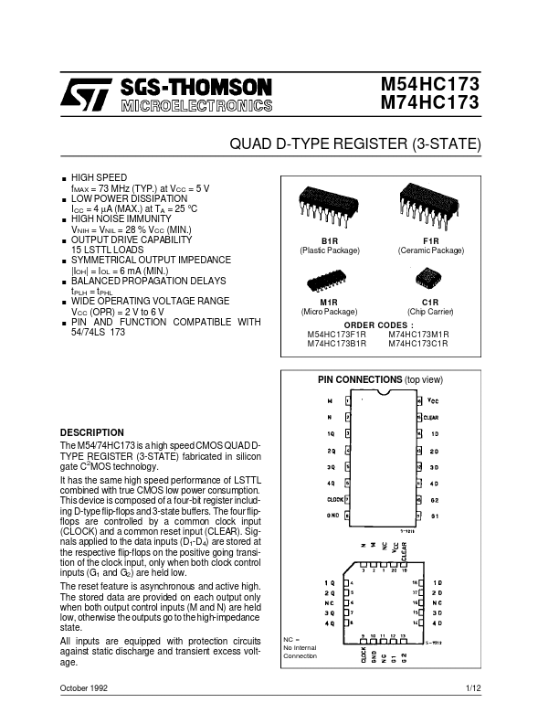
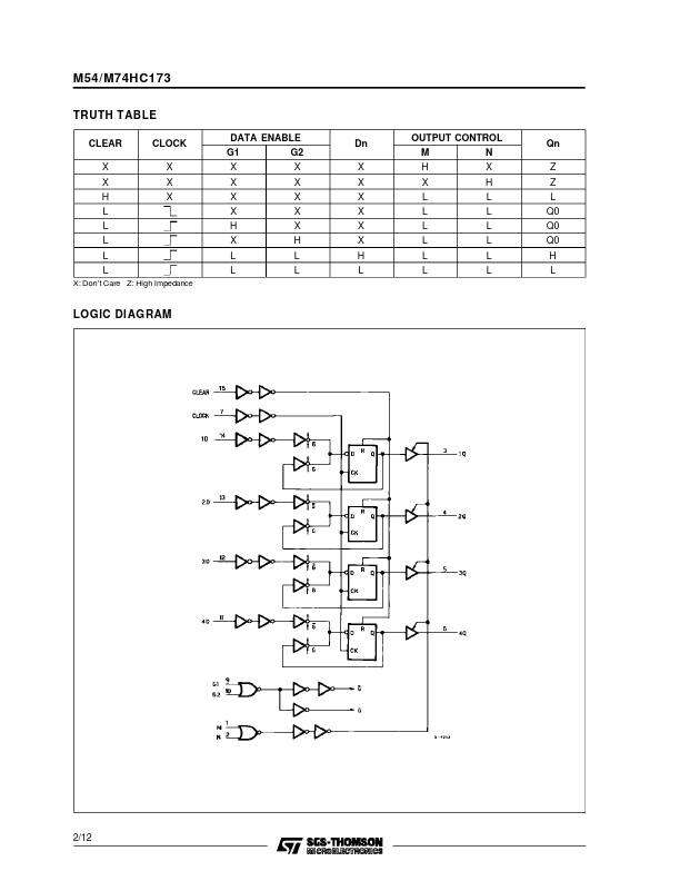
The four flipflops are controlled by a common clock input (CLOCK) and a common reset input (CLEAR). Signals applied to the data inputs (D1-D4) are stored at the respective flip-flops on the positive going transition of the clock input, only when both clock control inputs (G1 and G2) are held low. The reset feature is asynchronous and active high. The stored data are provided on each output only when both output control inputs (M and N) are held low, otherwise the outputs go to the high-impedance state. All inputs are equipped with protection circuits against static discharge and transient excess voltage. October 1992 NC = No Internal Connection 1/12 M54/M74HC173 TRUTH TABLE CLEAR X X H L L L L L X: Don’t Care Z: High Impedance CLOCK X X X DATA ENABLE G1 X X X X H X L L G2 X X X X X H L L Dn X X X X X X H L OUTPUT CONTROL M H X L L L L L L N X H L L L L L L Qn Z Z L Q0 Q0 Q0 H L LOGIC DIAGRAM 2/12 M54/M74HC173 INPUT AND OUTPUT EQUIVALENT CIRCUIT PIN DESCRIPTION
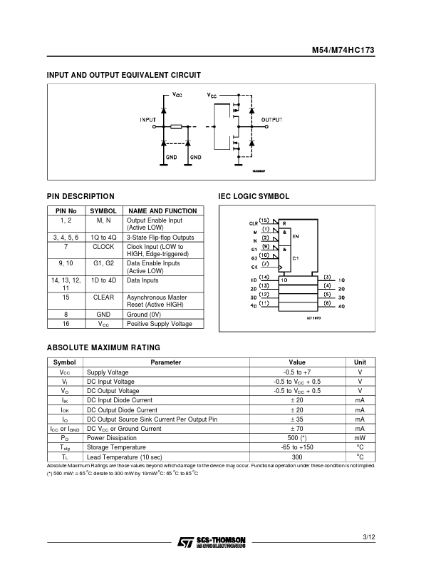
PIN No 1, 2 3... STMicroelectronics