DESCRIPTION
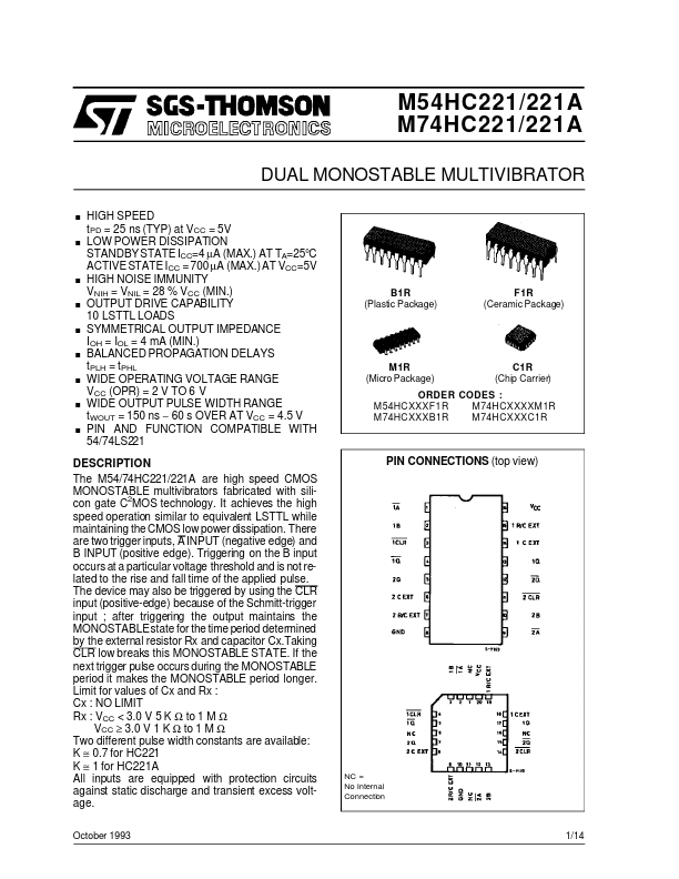
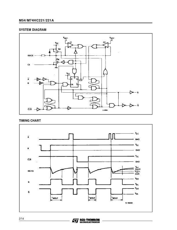
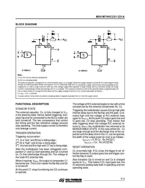
There are two trigger inputs, A INPUT (negative edge) and B INPUT (positive edge). Triggering on the B input occurs at a particular voltage threshold and is not related to the rise and fall time of the applied pulse. If the next trigger pulse occurs during the MONOSTABLE period it makes the MONOSTABLE period longer. Limit for values of Cx and Rx : Cx : NO LIMIT Rx : VCC < 3.0 V 5 K Ω to 1 M Ω VCC ≥ 3.0 V 1 K Ω to 1 M Ω Two different pulse width constants are available: K ≅ 0.7 for HC221 K ≅ 1 for HC221A All inputs are equipped with protection circuits against static discharge and transient excess voltage. October 1993 PIN CONNECTIONS (top view) NC = No Internal Connection 1/14 M54/M74HC221/221A SYSTEM DIAGRAM TIMING CHART 2/14 M54/M74HC221/221A BLOCK DIAGRAM Note : (1) Cx, Rx, Dx are external components. (2) Dx is a clamping diode. The external capacitor is charged to VCC inthe stand-by state, i.e. no trigger. When the supply voltage is turned off Cx is discharged mainly through an internal parasitic diode (see figures). STMicroelectronics