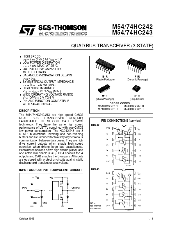
DESCRIPTION
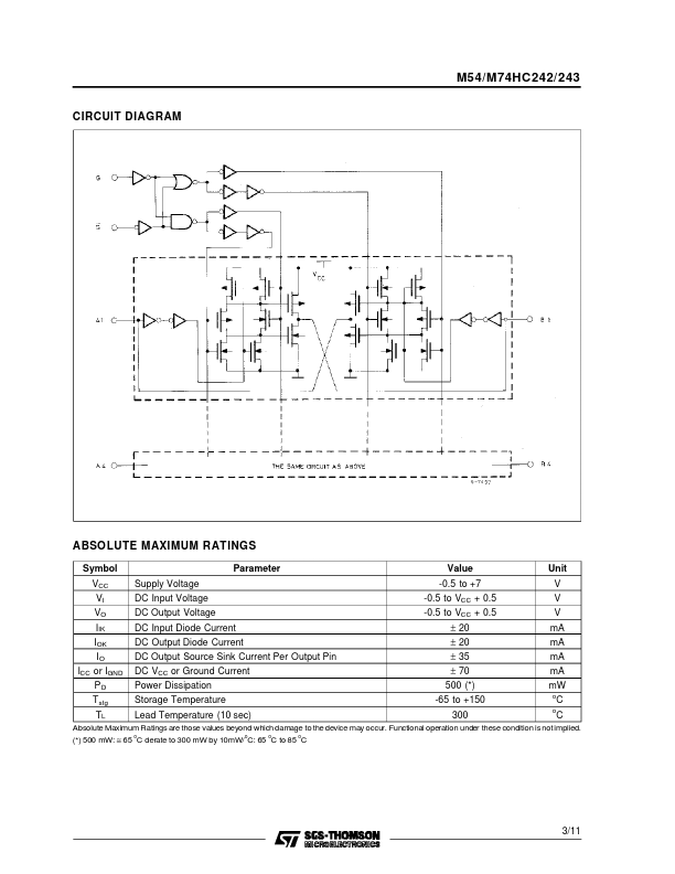
They are high drive current outputs which enable high speed operation when driving large bus capacitances. Each device has one active high enable (GBA), and one active low enable (GAB). GBA enables the A outputs and GAB enables the B outputs. All inputs are equipped with protection circuits against static discharge and transient excess voltage. INPUT AND OUTPUT EQUIVALENT CIRCUIT ORDER CODES : M54HCXXXF1R M74HCXXXM1R M74HCXXXB1R M74HCXXXC1R PIN CONNECTIONS (top view) HC242 HC243 NC = No Internal Connection October 1993 1/11 M54/M74HC242/243 CHIP CARRIER TRUTH TABLE INPUTS GAB GBA H L H L H L L H FUNCTION A BUS B BUS OUTPUT INPUT OUTPUTS HC242 HC243 A=B A=B B=A Z Z PIN DESCRIPTION
PIN No 1 2, 12 3, 4, 5, 6 11, 10, 9, 8 13 7 14 SYMBOL GAB NC 1A to 4A 1B to 4B GBA GND VCC NAME AND FUNCTION Output Enable Input (active LOW) Not connected Data Inputs/Outputs Data Inputs/Outputs Output Enable Input Ground (0V) Positive Supply Voltage INPUT OUTPUT B = A HIGH IMPEDANCE Z HIGH IMPEDA... STMicroelectronics