DESCRIPTION
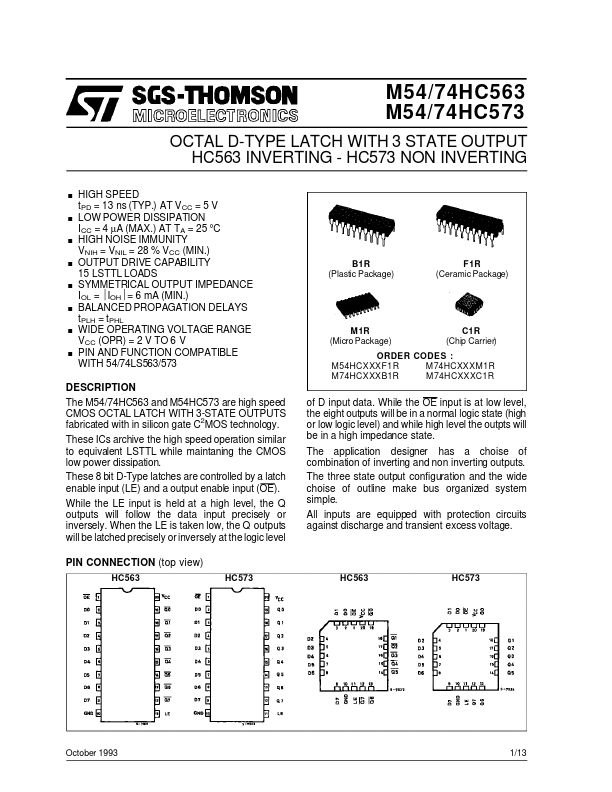
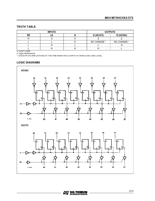
While the LE input is held at a high level, the Q outputs will follow the data input precisely or inversely. When the LE is taken low, the Q outputs will be latched precisely or inversely at the logic level PIN CONNECTION (top view) HC563 HC573 of D input data. While the OE input is at low level, the eight outputs will be in a normal logic state (high or low logic level) and while high level the outpts will be in a high impedance state. The application designer has a choise of combination of inverting and non inverting outputs. The three state output configuration and the wide choise of outline make bus organized system simple. All inputs are equipped with protection circuits against discharge and transient excess voltage. HC563 HC573 October 1993 1/13 M54/M74HC563/573 INPUT AND OUTPUT EQUIVALENT CIRCUIT PIN DESCRIPTION
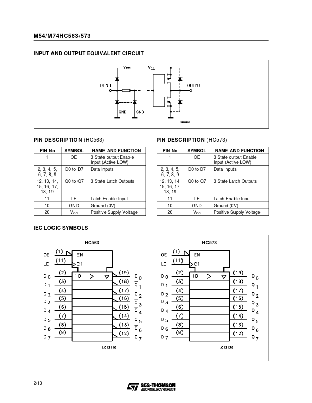
(HC563) PIN No 1 2, 3, 4, 5, 6, 7, 8, 9 12, 13, 14, 15, 16, 17, 18, 19 11 10 20 SYMBOL OE D0 to D7 Q0 to Q7 NAME AND FUNCTION 3 State output Enable Input (A... STMicroelectronics