STMicroelectronics M54HCT75
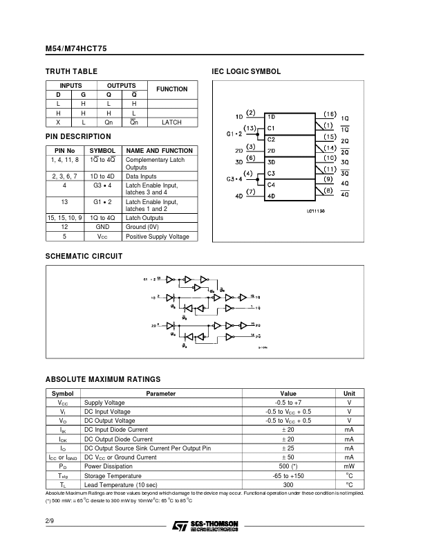
The data applied to the data input is transfered to the Q and Q outputs when the enable input is taken high and the outputs will follow the data input as long as the enable input is kept high. When the enable input is taken low, the information data applied to the data input isretained atthe outputs.| Part No. | M54HCT75 |
|---|---|
| Datasheet | M54HCT75 Download |
| Manufacturer |  STMicroelectronics |
| Description | 4 BIT D TYPE LATCH |
| Buy | Stock & Price |
DESCRIPTION
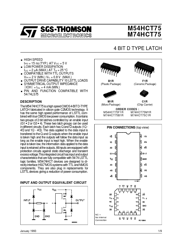
TheM54/74HCT75 isahigh speedCMOS4-BITD-TYPE LATCH fabricated in silicon gate C2MOS technology. It has the same high speed performance of LSTTL combined withtrueCMOSlow power consumption. Itcontains two groups of 2-bit latches controlled by an enable input (G1● 2 or G3
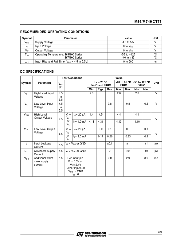
● 4). These two latch groups can be used indifferent circuits. Each latch has Q and Q outputs (1Q 4Q and 1Q - 4Q). All inputs areequipped with protection circuits against static discharge and transient excessvoltage.This integrated circuit has input andoutput characteristics that are fully compatible with 54/74 LSTTL logic families. M54/74HCT devices are designed to directly interface HSC2MOS systems with TTL and NMOS components. They are also plug in replacements for LSTTL devices giving a reduction of power consumption. M1R (Micro Package) C1R (Chip Carrier) ORDER CODES : M54HCT75F1R M74HCT75M1R M74HCT75B1R M74HCT75C1R PIN CONNECTIONS (top view) INPUT AND OUTPUT EQUIVALENT CIRCUIT NC = No Internal Connectio...