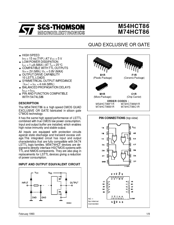
DESCRIPTION
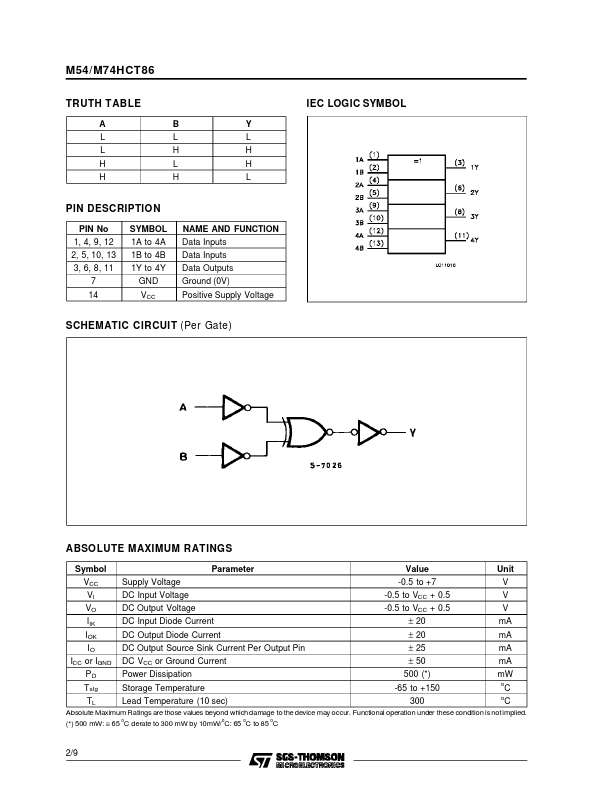
Input and output buffer are installed, which enables high noise immunity and stable output. All inputs are equipped with protection circuits against static discharge and transient excess voltage.This integrated circuit has input and output characteristics that are fully compatible with 54/74 LSTTL logic families. M54/74HCT devices are designed to directly interface HSC2MOS systems with TTL and NMOS components. They are also plug in replacements for LSTTL devices giving a reduction of power consumption. INPUT AND OUTPUT EQUIVALENT CIRCUIT ORDER CODES : M54HCT86F1R M74HCT86M1R M74HCT86B1R M74HCT86C1R PIN CONNECTIONS (top view) NC = No Internal Connection February 1993 1/9 M54/M74HCT86 TRUTH TABLE A L L H H B L H L H Y L H H L IEC LOGIC SYMBOL PIN DESCRIPTION
PIN No 1, 4, 9, 12 2, 5, 10, 13 3, 6, 8, 11 7 14 SYMBOL 1A to 4A 1B to 4B 1Y to 4Y GND VCC NAME AND FUNCTION Data Inputs Data Inputs Data Outputs Ground (0V) Positive Supply Voltage SCHEMATIC CIRCUIT (Per Gate) ABSOLUTE M... STMicroelectronics