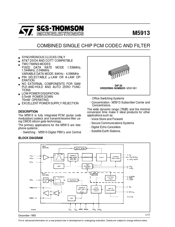
DESCRIPTION
December 1993 1/17 This is advanced information on a new product now in development or undergoing evaluation. Details are subject to change without notice. M5913 ABSOLUTE MAXIMUM RATINGS
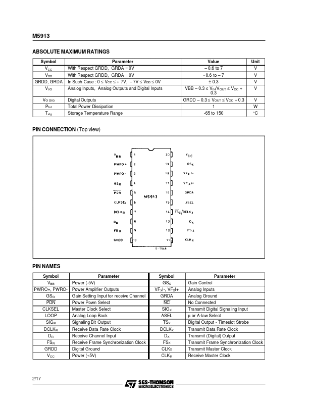
Symbol VCC VBB GRDD, GRDA VI/O VO DIG Ptot Tstg Parameter With Respect GRDD, GRDA = 0V With Respect GRDD, GRDA = 0V In Such Case : 0 ≤ VCC ≤ + 7V, – 7V ≤ VBB ≤ 0V Analog Inputs, Analog Outputs and Digital Inputs Digital Outputs Total Power Dissipation Storage Temperature Range Value – 0.6 to 7 - 0.6 to – 7 ± 0.3 VBB – 0.3 ≤ VIN/VOUT ≤ VCC + 0.3 GRDD – 0.3 ≤ VOUT ≤ VCC + 0.3 1 -65 to 150 Unit V V V V V W °C PIN CONNECTION (Top view) PIN NAMES Symbol VBB PWRO+, PWROGSR PDN CLKSEL LOOP SIG R DCLKR DR FSR GRDD VCC Power (-5V) Power Amplifier Outputs Gain Setting Input for receive Channel Power Pown Select Master Clock Select Analog Loop Back Signaling Bit Output Receive Data Rate Clock Receive Channel Input Receive Frame Synchronization Clock Digital Ground Power (+5V) Parameter Symbol GSX VFXI... STMicroelectronics