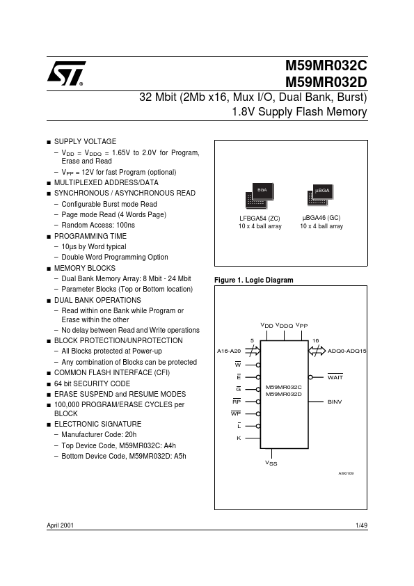
DESCRIPTION
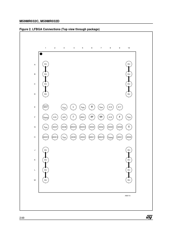
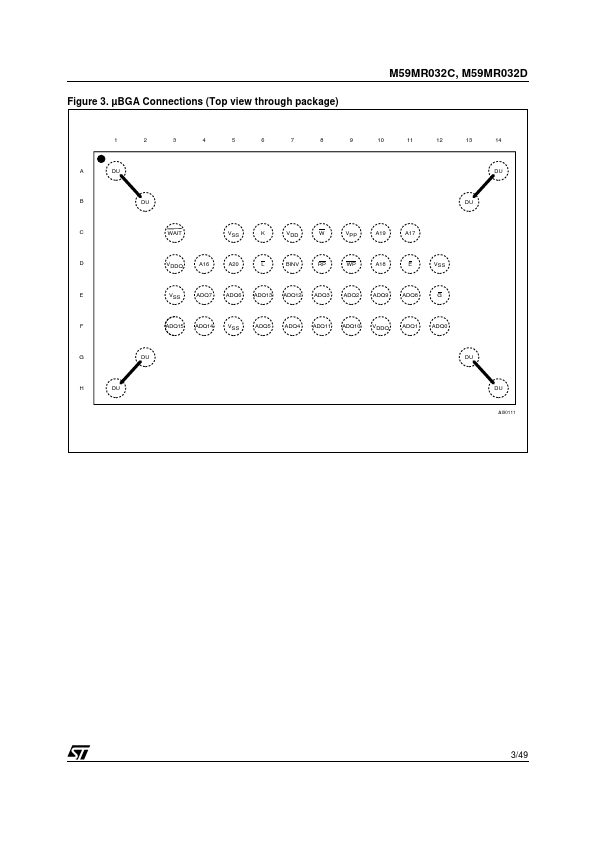
In synchronous burst mode, a new data is output at each clock cycle for frequencies up to 54MHz. The array matrix organization allows each block to be erased and reprogrammed without affecting other blocks. All blocks are protected against programming and erase at Power-up. Blocks can be unprotected to make changes in the application and then reprotected. Instructions for Read/Reset, Auto Select, Write Configuration Register, Programming, Block Erase, Bank Erase, Erase Suspend, Erase Resume, Block Protect, Block Unprotect, Block Locking, CFI Query, are written to the memory through a Command Interface (C.I.) using standard microprocessor write timings. The memory is offered in LFBGA54 and µBGA46, 0.5 mm ball pitch packages and it is supplied with all the bits erased (set to ’1’). Table 2. ABSOLUTE MAXIMUM RATINGS
(1) Symbol TA TBIAS TSTG VIO (3) VDD, VDDQ VPP Parameter Ambient Operating Temperature (2) Temperature Under Bias Storage Temperature Input or Output Voltage Supply Voltage Program Voltage Value –40 to 85 –40 to 125 –55 to 155 –0.5 to VDDQ+0.5 –0.5 to 2.7 –0.5 to 13 Unit °C °C °C V V V Note: 1. STMicroelectronics