DESCRIPTION
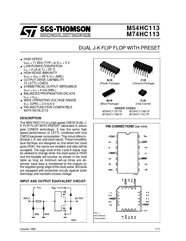
This circuit offers individual J, K, set, and clock inputs. These monolithic dual flip-flops are designed so that when the clock goes HIGH, the inputs are enabled and data will be accepted. The logic level of the J and K inputs may be allowed to change when the clock pulse is HIGH and the bistable will function as shown in the truth table as long as minimum set-up times are observed. Input data is transferred to the outputs on the negative-going edge of the clock pulse. All inputs are equipped with protection circuits against static discharge and transient excess voltage. INPUT AND OUTPUT EQUIVALENT CIRCUIT PIN CONNECTIONS (top view) NC = No Internal Connection October 1992 1/11 M54/M74HC113 TRUTH TABLE INPUTS PR L H H H H H X: Don’t Care OUTPUTS K X L H L H X CK X Q H Qn L H Qn Qn Q L Qn H L Qn Qn J X L L H H X FUNCTION PRESET NO CHANGE TOGGLE NO CHANGE LOGIC DIAGRAM 2/11 M54/M74HC113 PIN DESCRIPTION
PIN No 1, 13 2, 12 3, 11 4, 10 5, 9 6, 8 7 14 SYMBOL 1CK, 2CK 1K, 2K 1J,... STMicroelectronics